1
Other Equipment & Products / Re: Crimpin’ ain’t easy (or: best hobbyist crimping tool/system?)
« Last post by watchmaker on Today at 12:44:51 pm »Is IWISS getting better? Look at the polish.


 Recent Posts
The tap changer could be powered from the same supply as the LM723 if the tap changer is modified to input negative sensing voltage.Initial thoughts are, the fans only can be powered from the 2x15Vac transformer.
The tap changer might be able to be powered from the 2x12Vac transformer with modifications so that it can accept negative sensing input voltage. Because the DVM can only measure positive voltage, it needs to be powered WRT the PSU's negative output. So the unmodified tap changer might as well be powered from the same supply.
Keep in mind that ground on a Harrison PSU is the positive output.
Can you please be more explicit ? Are you trying to explain that the tap changer could be powered if I modify the schematic ? Regarding the DVM, I didn't understood.
Oscilloscopes are for displaying signal waveforms, not creating them.
They describe it as "chopper stabilized" in the datasheet. If you think about it, the part S1, gm1, gm2, S2 is a chopper amplifier: S1 chops the differential input voltage into a square wave, the linear transistors amplify the square wave, and S2 demodulates it back into DC by sampling the peaks. To avoid differential subtraction of peaks and valleys at this point, gm3 works as a DC servo of sorts and ensures that the valleys are fixed near some internal "ground" potential.
The output of the chopper feeds gm4 and gm5, which provide additional gain. And the whole chopper is bypassed at frequencies near the chopping frequency and above in order to reduce aliasing artifacts and achieve GBW much higher than the chopping frequency.
Of course the "auto zero" explanation about gm3 canceling gm1 offset voltage and a bunch of sample-and-hold circuits making it all work is valid too. I'm not sure what the difference between "chopper stabilized" and "auto zero" is supposed to be, and if there is any real difference at all. Maybe it's only marketing talk.

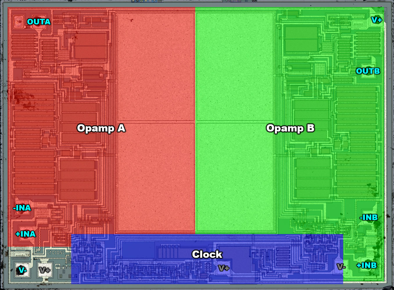
It's probably same thing as with MCP6024: two dual dice can be installed together to realize a quad. The top die gets its V+ in bottom left and V- in bottom right. The bottom die is rotated 180° so its supply connections are swapped.
There are three unused bondpads in the lower area. These are additional options for connecting the supply potentials.
I suppose it works out cheaper than designing a quad die and disabling half of it for the dual

The circuit corresponds to the block diagram in the LTC1052 datasheet. The datasheet states that the amplification factors of the amplifiers gm1 and gm6 must be as equal as possible for proper function. Furthermore, these are the amplifier stages with the high amplification factors. Accordingly, these two sections are relatively large and have the same structure.These things look like ordinary PMOS differential pairs with PMOS current sources in the middle between gm1 and gm6 and NMOS current mirrors.
Hmm, how far are you from a complete transistor level schematic of this opamp?
Why do you think that builder is using it? Just curious your thoughts on it. He (or she) doesn't seem like a person to make a mistake like that.The builder is using CA glue. What's wrong with what he chose, seems to know what he's doing. You can use SCIGrip 16 if you don't want to use that.
CA glue is a bad choice for pvc

The builder is using CA glue. What's wrong with what he chose, seems to know what he's doing. You can use SCIGrip 16 if you don't want to use that.