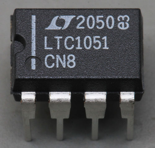
The LTC1051 contains two so-called zero-offset opamps. Originally, attempts were only made to optimise the offset voltage and offset drift of opamps with circuit technology and better semiconductor processes. In addition, there is often an adjustment during the manufacture of the components. Initially, only resistors were adjusted for this purpose. This was done either by trimming with a laser or by activating or deactivating resistors via fuses. Well you probably know all this.

Nowadays, some opamps contain memory that gets correction values during production and then does the offset correction in the circuit.
Zero-offset opamps, on the other hand, are constantly correcting their current offset. There are two techniques for this. Auto-zero opamps work according to a sample & hold principle in which offset voltages are determined cyclically and then used for correction. Chopper opamps modulate and demodulate the signal. In practice, switch groups at the input and output of the opamp usually exchange the signal crosswise. Correctly implemented, this compensates for the offset voltage. The real implementations are sometimes very different and there are also combinations of the two techniques. The terms are often mixed up or used incorrectly.
Zero-offset opamps offer exceptional offset values. They are usually also more robust against interference from the power supply. The challenges are the additional analogue switches in the signal path. Depending on the circuit, additional capacitors are required whose properties are critical. Depending on the concept, additional high-frequency interference occur in the switching frequency range. There can be mixed frequency products or the noise density increases at low frequencies.
The offset voltage of the LTC1051 is typically +/-0,5µV, maximum +/-5µV. The average temperature drift is typically specified as 0µV/°C and can be a maximum of +/-0,05µV/°C. To keep the noise as low as possible, zero-offset opamps often consume a little more supply current. For the LTC1051, 1mA per opamp is specified. The datasheet specifies the cut-off frequency as typically 2,5MHz. The maximum slew rate is 4V/µs.

The advert above was published in the magazine EDN in 1990. It shows the different variants of this opamp family. Here the opamps are referred to as "choppers". In the datasheet of the TLC1051, the categorisation is less clear, but a proximity to chopper opamps is always suggested. The TLC1052 is clearly labelled as a chopper opamp in its datasheet.
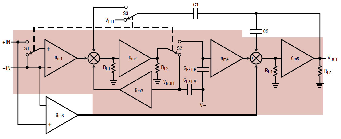
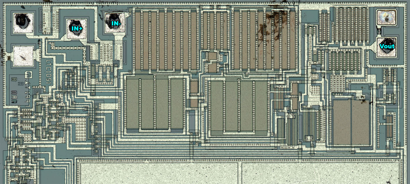
The datasheet for the TLC1051 does not contain any details on how it works. Sample & hold capacitors are mentioned repeatedly. As will be shown later, the architecture of the TLC1051 corresponds to the TLC1052, whose datasheet contains a block diagram. In the TLC1051, the capacitors Ca and Cb are only integrated, whereas in the TLC1502 they have to be added externally.
This shows that the TLC1051 is not a chopper amplifier but an auto-zero opamp. The signal does not undergo modulation and demodulation. Instead, the current offset value is stored in a capacitor and used for correction, while another capacitor holds the current value of the signal. In addition to the auto-zero path, the TLC1051 includes a parallel path for higher frequencies. This type of opamp is referred to as "auto-zero stabilised".
If the switches are in the position shown above, the inputs of amplifier gm1 are short-circuited. This amplifier usually has a high amplification factor so that it is sufficient to compensate its offset voltage. The capacitor Ca stores the value of the amplified offset voltage. In the second phase all switches are switched. The amplifier gm1 now processes the input signal. The output signal of the amplifier gm1 contains its amplified offset voltage. This offset voltage is stored in capacitor Ca and is subtracted via amplifier gm3. The amplified zero-offset signal is buffered via the amplifier gm2 and loaded into the capacitor Cb, the sampling capacitor. The amplifier gm4 is another buffer amplifier. Amplifier gm5 is the output buffer.
The signal must not contain any high frequency components. The sampling process generates mixed frequencies. If frequencies are fed in that are close to the sampling frequency, the mixed products are particularly annoying. The gm6 amplifier with capacitors C1 and C2 provides a parallel path for high frequency signal components and fulfils two tasks in this context. Firstly, the gm6 amplifier ensures that the LTC1051 can also process higher frequencies. At the same time, the high frequency path prevents the higher frequencies from reaching the sampling circuit. At high frequencies, a current flows through capacitor C1, reducing the input level at amplifier gm2 and thus the amplification factor of the auto-zero path.
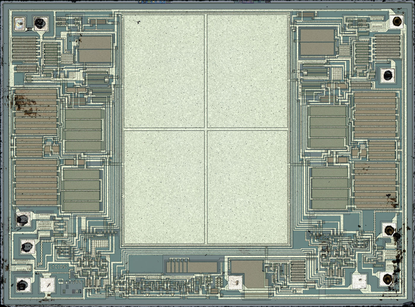
The die is relatively large, measuring 3,4mm x 2,5mm. This image is available in higher resolution:
https://www.richis-lab.de/images/Opamp/89x04XL.jpg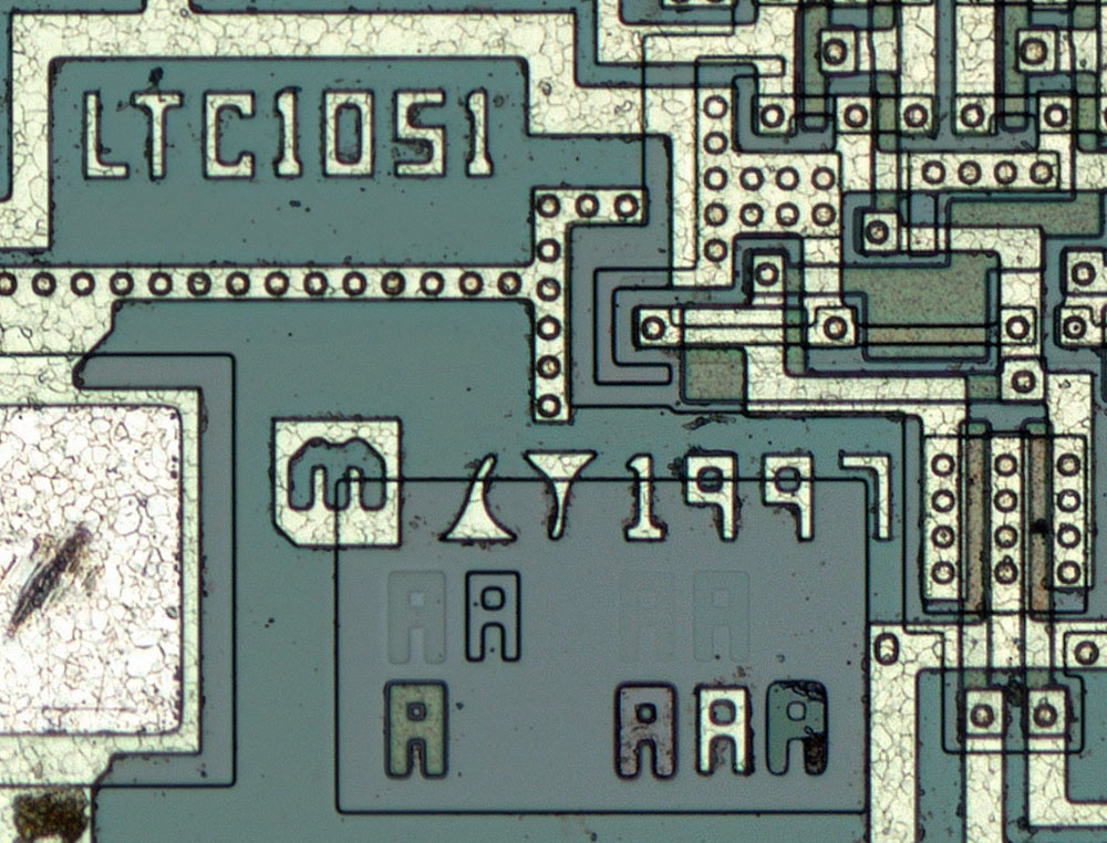
The design obviously dates back to 1997 and the revisions of eight masks can also be recognised. The fact that this opamp family was advertised as early as 1990 and the masks all have an A revision suggests that the design has been completely revised in the meantime.
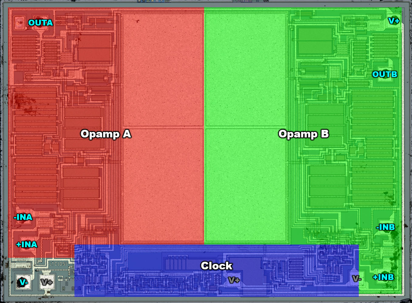
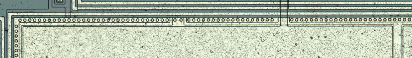
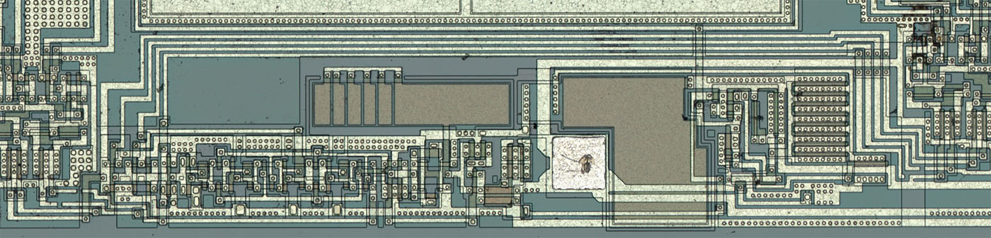
The two opamps have a relatively symmetrical design. The capacitors, which have to be connected externally on the LTC1052, take up a large part of the area. The clock generator is integrated in the lower area of the die.
There are three unused bondpads in the lower area. These are additional options for connecting the supply potentials. The bondpad in the top left-hand corner is connected to a testpad via a fuse. What exactly this fuse could be used for remains unclear.
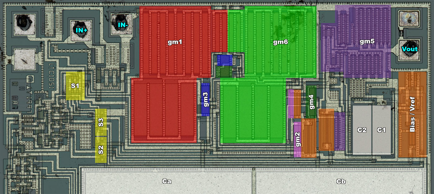
The circuit corresponds to the block diagram in the LTC1052 datasheet. The datasheet states that the amplification factors of the amplifiers gm1 and gm6 must be as equal as possible for proper function. Furthermore, these are the amplifier stages with the high amplification factors. Accordingly, these two sections are relatively large and have the same structure.
The large capacitors obviously consist of three layers in order to maximise capacitance.
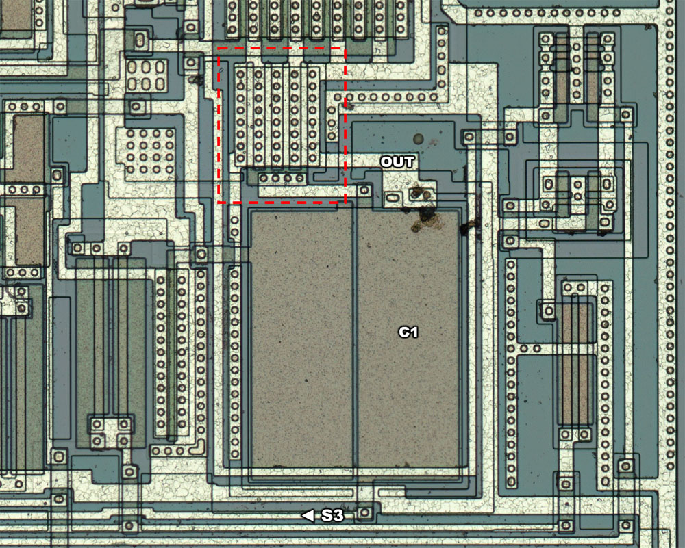
The datasheet emphasises that capacitors C1 and C2 must be as identical as possible. For this reason, it is very surprising that there is a large MOSFET in parallel with capacitor C1, which only represents an additional capacitance. Perhaps this is intended to compensate for a parasitic capacitance at another point.
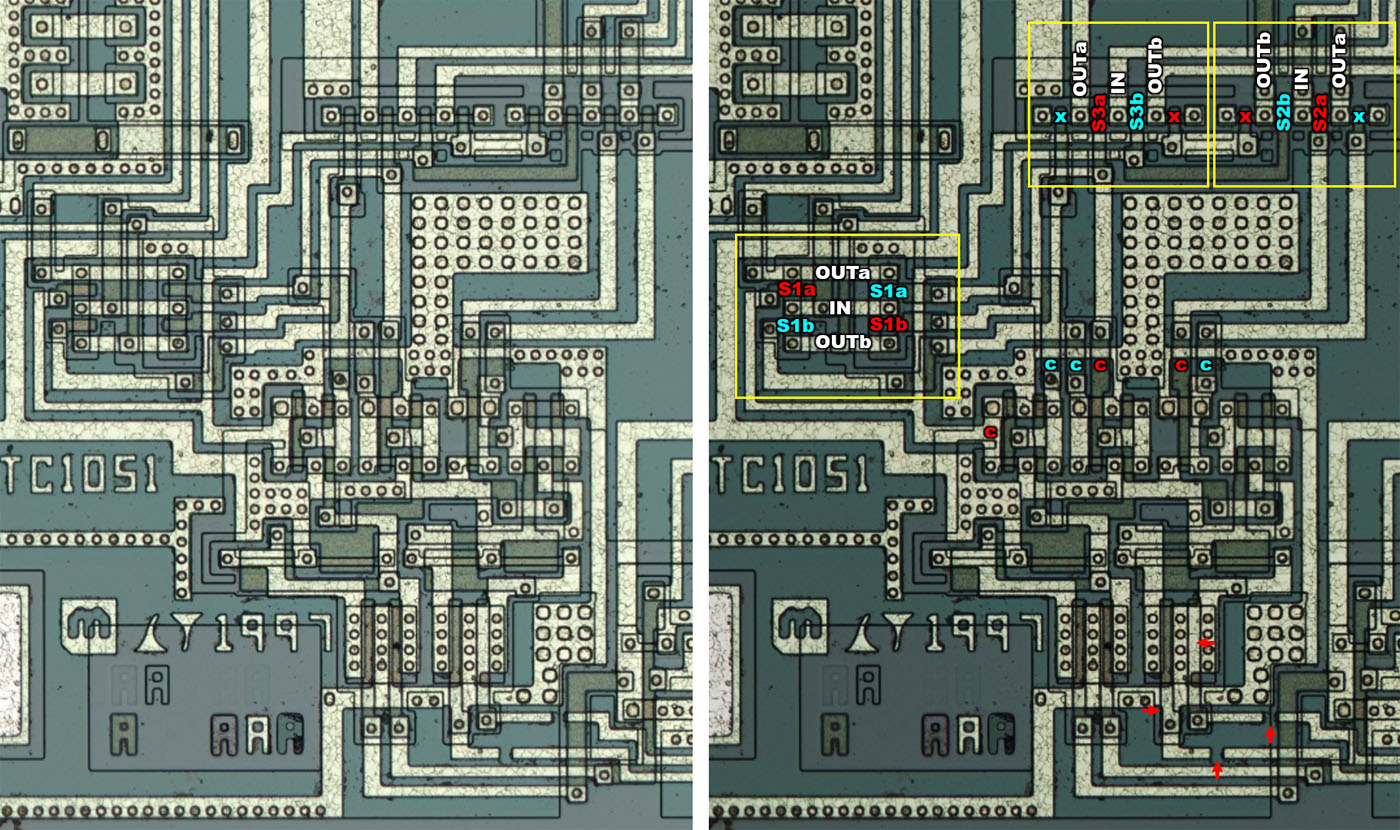
Four clock signals are generated in the clock generator. Two of these clock signals serve as the basis for generating the control signals for both opamps. The other two clock signals are not used, but are nevertheless routed to both opamps. The lines are then interrupted there. The transistors that would receive the alternative clock signals are connected to the supply potentials.
The control circuit consists of two very similar blocks that are connected in the centre. They generate a total of six control signals ("c"). The colours show which control signals have at least a similar phase. The switches with the letter "a" realise the upper switch position in relation to the block diagram.
At the input, the changeover switch S1 is doubled in order to represent an analogue switch that is as ideal as possible with PMOS and NMOS transistors connected in parallel. Switches S2 and S3 provide additional switches on the right and left which are not used. Obviously, some options have been kept open here in order to adapt the switching behaviour.
The clock generator is divided in two parts. The clock is generated on the right of the bondpad and processed on the left of the bondpad. The large capacitor on the left makes it possible to adjust the effective capacitance via the connections in the metal layer. This probably allows the duty cycle to be adjusted. This would be plausible, as a sufficient dead time must be maintained when throwing the switches.
https://www.richis-lab.de/Opamp85.htm 


 Recent Posts