Great photos!
Undesired recombination at the Si SiO2 interface will produce IR. That IR emission is used to find trouble spots.
Standard recombination in GaxAl1-xAs produces quite a bit of light since the dominant mechanism is optical emission. The color typically ranges from IR to red depending on the composition.
Light emission due to avalanche breakdown in GaAs is typically green.
Thanks!

SiC glows blue. Looks really nice!

Unfortunately I have no pictures of SiC-semiconductors...
Hi all!
Let´s take a look at a newer BUX22!


Well that´s a big heatspreader! It was necessary because the base plate of the package is thinner than the old generation (
https://richis-lab.de/Bipolar07.htm).

You can already see the thickness of the metal layer.
The BUX22 makes use of a perforated emitter. The die has a MESA-structure.


And of course second breakdown.

More pictures here:
https://richis-lab.de/Bipolar08.htm 
I wonder why using two dies? As I see, both dies are in parallel without any balansing resistors. They must be very well matched, and, from the secondary breakdown pic, it looks like they are.
I also noticed a few red spots outside where they shouldn't be. I wonder what's that. Like, the one on the right die near the bottom pad.
I wonder why using two dies? As I see, both dies are in parallel without any balansing resistors. They must be very well matched, and, from the secondary breakdown pic, it looks like they are.
Two smaller dies result in a better production yield than one big die.
And with two smaller dies you can use the same die but one for a smaller transistor.
I also noticed a few red spots outside where they shouldn't be. I wonder what's that. Like, the one on the right die near the bottom pad.
These are high iso pictures. There are some noise pixels…
I wonder why using two dies? As I see, both dies are in parallel without any balansing resistors. They must be very well matched, and, from the secondary breakdown pic, it looks like they are.
I also noticed a few red spots outside where they shouldn't be. I wonder what's that. Like, the one on the right die near the bottom pad.
If a high power die is getting too large, temperature in the center is getting too high compared to the boundary due to limited heat conductance.
Not a problem for a 2N3055, but real for a BUX22.
Not reeeeally... I've seen single MOSFET and IGBT dies bigger than the inside area of a TO-3. More likely it was contemporary yields.
Don't know what the largest BJT die is, these days; might not even be one as large, just because there's so little demand for them.
Tim
Not reeeeally... I've seen single MOSFET and IGBT dies bigger than the inside area of a TO-3. More likely it was contemporary yields.
Don't know what the largest BJT die is, these days; might not even be one as large, just because there's so little demand for them.
Tim
Same problem with MOSFETs. IXYS uses graded threshold voltages to tackle this problem (high threshold in the center) for their linear MOSFETSs.
All others - same story, with hotspotting in linear mode. See NASA, Spirito Effect.
I wonder why using two dies? As I see, both dies are in parallel without any balansing resistors. They must be very well matched, and, from the secondary breakdown pic, it looks like they are.
I also noticed a few red spots outside where they shouldn't be. I wonder what's that. Like, the one on the right die near the bottom pad.
We could drill out the remaining pin hole, and get a cheap matched pair transistor?

Not reeeeally... I've seen single MOSFET and IGBT dies bigger than the inside area of a TO-3. More likely it was contemporary yields.
Don't know what the largest BJT die is, these days; might not even be one as large, just because there's so little demand for them.
Tim
Same problem with MOSFETs. IXYS uses graded threshold voltages to tackle this problem (high threshold in the center) for their linear MOSFETSs.
All others - same story, with hotspotting in linear mode. See NASA, Spirito Effect.
The "reeeeally" being, most transistors that size are made for switching, so may have awful SOAs. The power dissipation is there, no contest, just doing it at voltage is harder.
That said, many newer MOSFETs, and even some IGBTs, are specified with DC SOA. However they've approached it -- graded threshold, tempco hackery, ballasting*, whatever -- it's done the trick.
*Probably not that, because source/emitter degeneration would severely eat into the saturated performance.
Tim
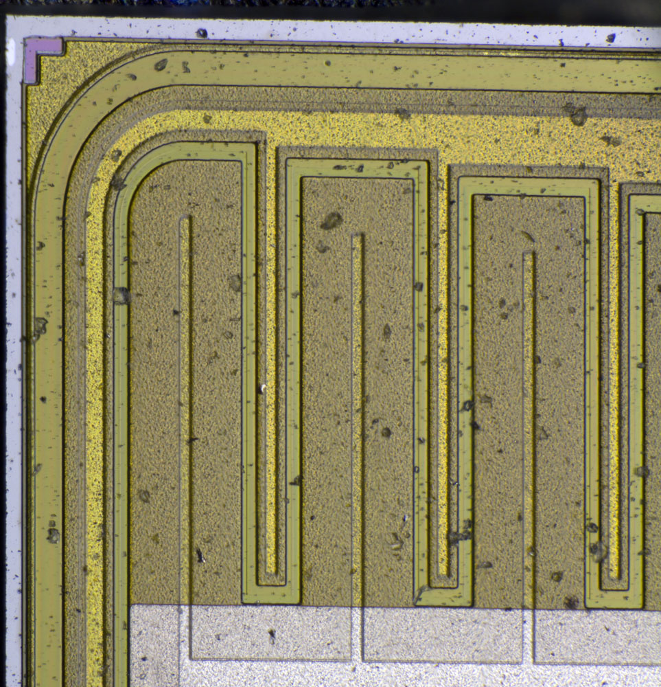
Did you know these small emitter contacts are called "wide-emitter narrow-contact"?
These structures make sure the current is evenly distributed. I assume that´s one reason why it was no bigger problem to connect the two dies in parallel.
Not reeeeally... I've seen single MOSFET and IGBT dies bigger than the inside area of a TO-3. More likely it was contemporary yields.
Don't know what the largest BJT die is, these days; might not even be one as large, just because there's so little demand for them.
Tim
Same problem with MOSFETs. IXYS uses graded threshold voltages to tackle this problem (high threshold in the center) for their linear MOSFETSs.
All others - same story, with hotspotting in linear mode. See NASA, Spirito Effect.
The "reeeeally" being, most transistors that size are made for switching, so may have awful SOAs. The power dissipation is there, no contest, just doing it at voltage is harder.
That said, many newer MOSFETs, and even some IGBTs, are specified with DC SOA. However they've approached it -- graded threshold, tempco hackery, ballasting*, whatever -- it's done the trick.
*Probably not that, because source/emitter degeneration would severely eat into the saturated performance.
Tim
Emitter ballasting is actually used, e.g., in high performance audio and, of course, RF power bipolar. More or less all "wide SOAR" stuff. Saturation voltage is of no concern there, and the drop along these resistors does not need to be large to equalize. Linear MOSFETS use the same trick at the source, among others, their RdsON is not as good as their switching cousins for the same reason.
Today the last one of the BUX22-trilogy:


Yeah, pretty sure a fake.

How did they cut the heatspreader?


Someone has lost a solder ball.


Quite interesting MESA-structure!

And here all three of them.
More pictures here:
https://richis-lab.de/Bipolar09.htm
I don't believe I've ever seen two dice paralled as in the BUX22 above. Looking at a data sheet, I don't see anything calling that out. I expect the dice are matched before packaging. Any thoughts on the characteristics that make this possible? I could see that emitter ballasting would help.
I was thinking of other applications for a dual power BJT that have reasonably matched dice with perhaps the bases and emitters brought out separately. One thing would be simple current mirror with a current range up to a few amps, but the collectors would have to be electrically isolated from each other.
It was common with bipolar RF power parts of the first generation (BLX15, ...)
Its obviously cheaper to have a bigger die when you really command the technology. If you dont,
yield goes substantially down with die size.
I don't believe I've ever seen two dice paralled as in the BUX22 above. Looking at a data sheet, I don't see anything calling that out. I expect the dice are matched before packaging. Any thoughts on the characteristics that make this possible? I could see that emitter ballasting would help.
I assume this "wide-emitter narrow-contact" technique makes it possible to connect the two dice.
I have heard that the BUX22 can often be seen connected in parallel without ballast resistors. Perhaps the BUX22 is a somewhat special bipolar transistor.

Hi all!
I have started a 2N3055-page:
https://richis-lab.de/2N3055.htmLast one is a RCA 2N3055
H which should contain a hometaxial transistor.
https://richis-lab.de/2N3055_05.htm


The trench following the emitter electrode contains the base-emitter-junction as the pictures of the avalanche breakdown shows.

But I´m not sure about the plateau following the trench. That has to be the emitter material. But why didn´t they design the base feed line shorter? There is no reason for more resistance in the base circuit. Perhaps the manufacturing process was the reason...

I took some more pictures of a RCA 2N3055:
https://richis-lab.de/2N3055_02.htmI´m pretty sure you can see the difference between the hometaxial and the epitaxial structure:
2N3055H
Here you can see a trench and some "small hills". With a hometaxial construction you have to etch the emitter away to contact the base material.
The surface is uneven because it´s cut or grinded or whatever (mechanical).

2N3055
The surface is very smooth. The reason behind this is the epitactical growth of silicon that gives a much cleaner surface.
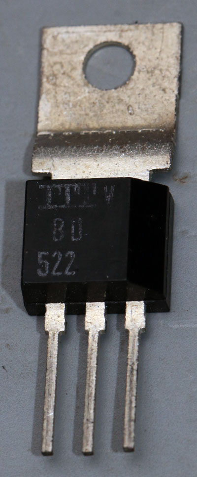
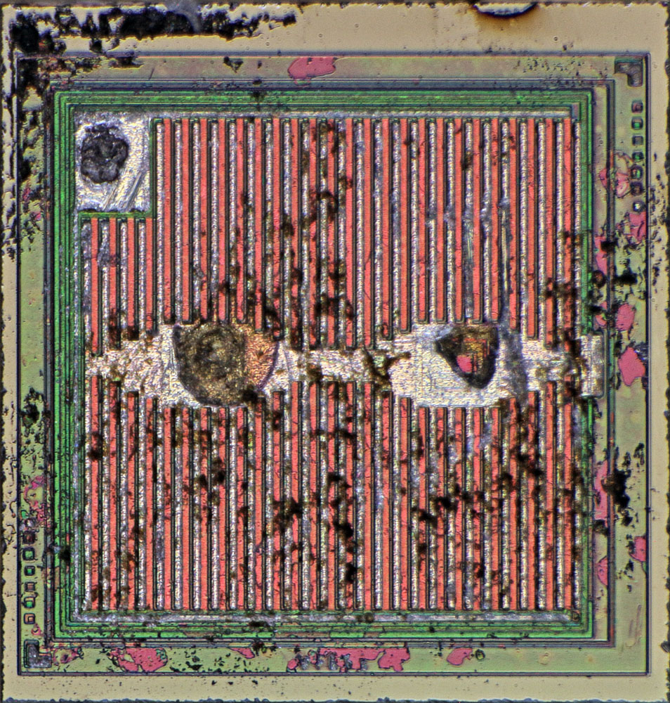
The BD522 looks like it's got eyes, LOL!

Today a new ST TIP3055:
https://richis-lab.de/Bipolar10.htm

Unfortunatelly the die didn´t survive in one piece but damage is not too bad.
I had only one try…

It uses a perforated emitter.
Thanks to exe for the part!
What's the thinking behind a perforated emitter?