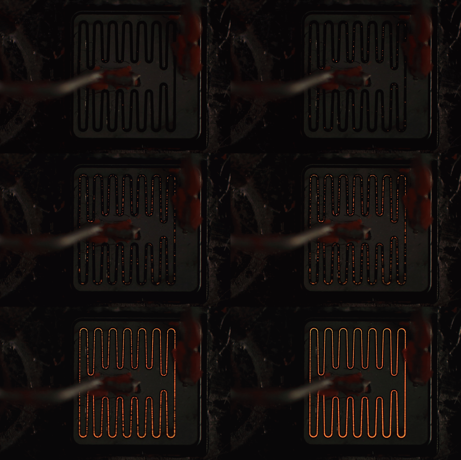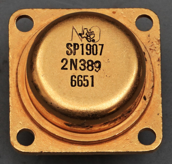
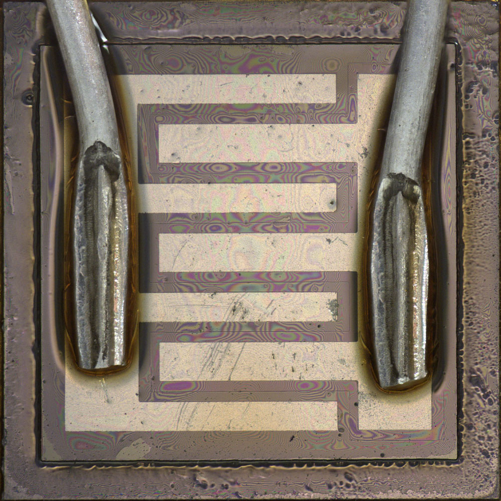
I once again took the 2N389 with its wide gap between the base and the emitter metallization and took some IR pictures...
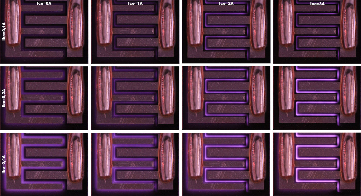
Compared with the SF137 here the base current is on the Y-axis and the collector current is on the X-axis. Without collector current, only the base region is illuminated, below which at the base-collector junction much of the recombination occurs. As the current increases, the light intensity increases.
At high base currents the luminous effect and thus most of the recombination shifts from the base area to the emitter area as the collector current increases. Here, the base current no longer flows via the collector to the emitter, but directly to the emitter in the base layer. At a base current of 0,4A and a collector current of 1A, the separation of base and emitter area can be seen nicely.
At low base currents (0,1A) and high collector currents (3A) the light is concentrated at the edges of the emitter surface. That´s were current crowding takes place, and a large part of the collector-emitter current flows through the edges. The transistor no longer operates in saturation here. In contrast to the SF137, the concentration of the luminance does not increase the brightness.
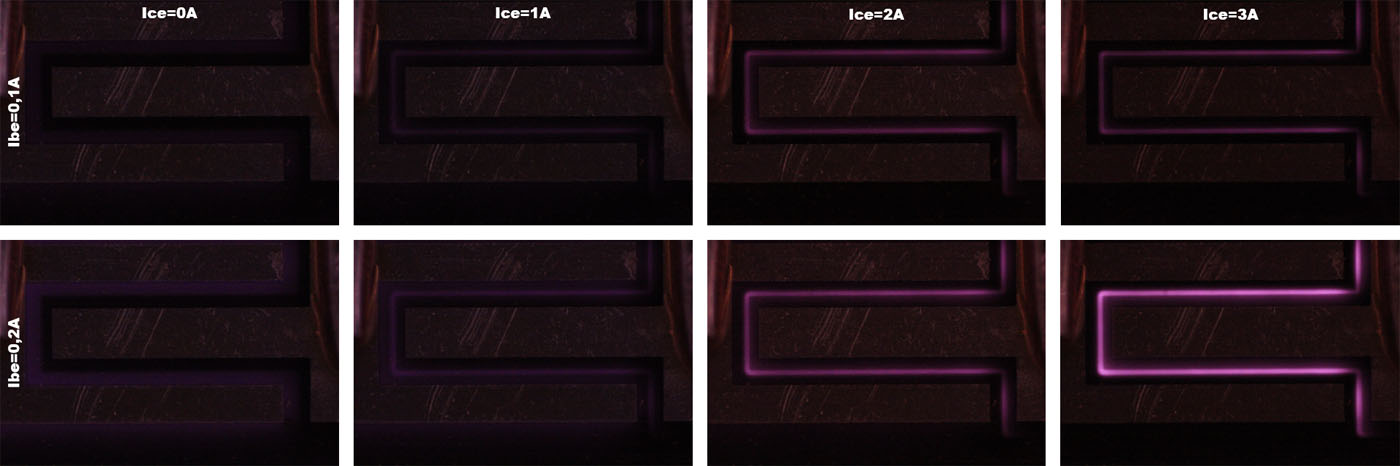
At a higher magnification, the images appear darker in particular. Otherwise, no other special features can be seen.
https://www.richis-lab.de/BipolarA09.htm#IR 
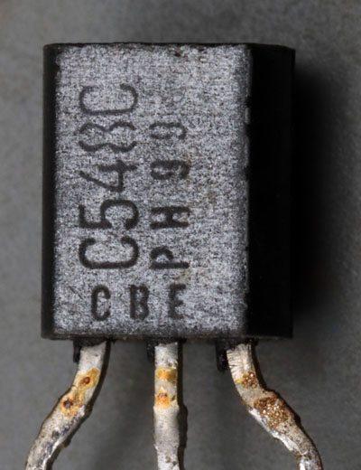
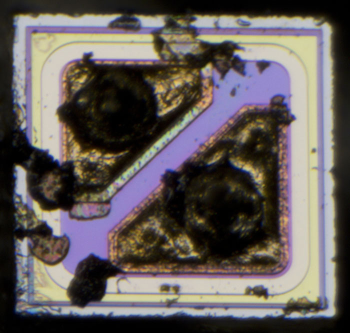
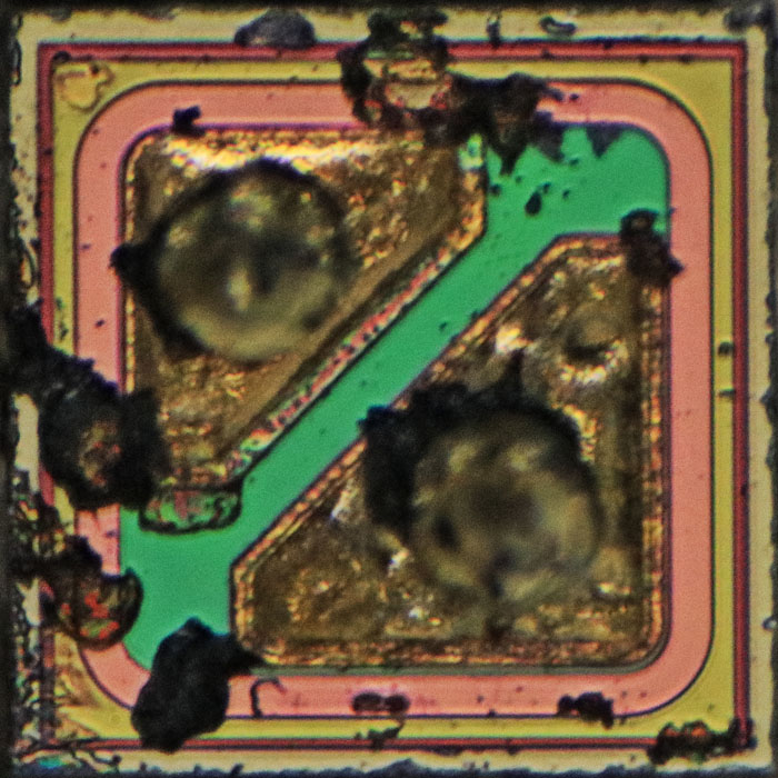
Just a small Philips BC548C...
Vce is a little lower than for the BC547C (https://www.richis-lab.de/Bipolar44.htm).
I always thought these were the same production but graded for Vce. My own tests with a curve tracer showed that the lower voltage versions often met the higher voltage breakdown specifications.
Just a small Philips BC548C...
Vce is a little lower than for the BC547C (https://www.richis-lab.de/Bipolar44.htm).
I always thought these were the same production but graded for Vce. My own tests with a curve tracer showed that the lower voltage versions often met the higher voltage breakdown specifications.
Perhaps they are the same production. Since I don't know how old these transistors are it is possible that we look at different generations.
I now have a BC section to clear the listing a little:
https://www.richis-lab.de/Transistoren_BC.htm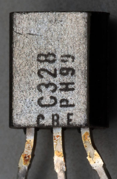
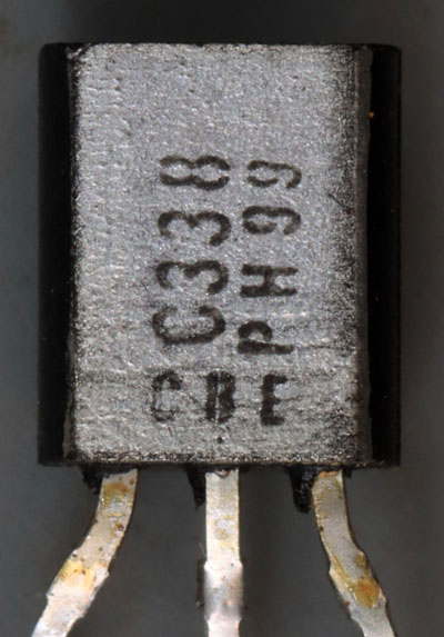
The Philips BC328 is a PNP transistor with a permanent current carrying capacity of 500mA, 1000mA is permissible for a short time. The BC328 blocks up to 25V. The cut-off frequency is 100MHz.
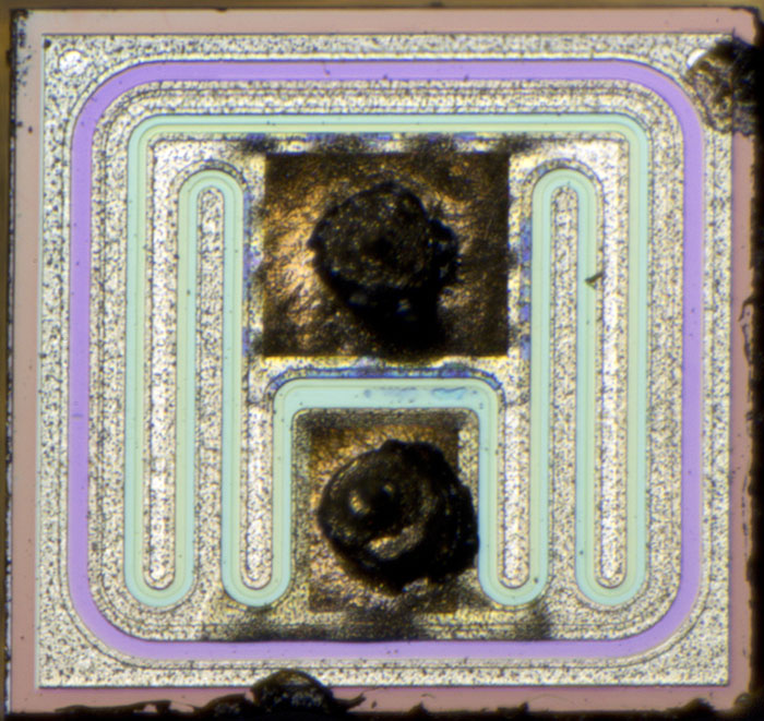
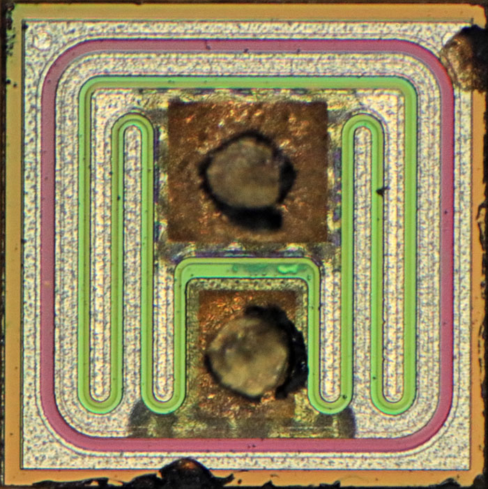
The die with an edge length of 0,57mm corresponds to the design of the MPSA56 (
https://www.richis-lab.de/Bipolar38.htm). Compared to other transistors of the BCxxx family, it is relatively large. That is necessary to achieve the specified current carrying capacity. For the same reason, there are relatively large interlocking metal contacts on the die, as we known them from power transistors.
https://www.richis-lab.de/BipolarA16.htm
Thanks!
I still have a big stockpile of pictures and parts too.


As usual: old and new, expensive and low-cost, bulky transistors and tiny complex wonder parts...
Is there a right way to open TO 220 to see the die? I want to compare both Chinese TDA2050 and LM1875.
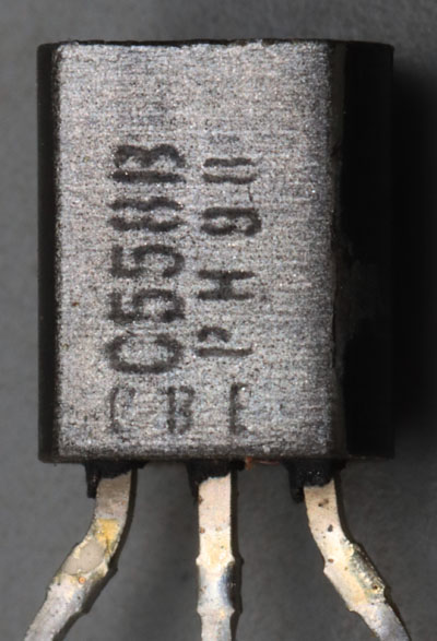
Another small old Philips transistor. The Philips BC558 PNP transistor has the same datasheet as the BC556. The BC558 is significantly less voltage resistant with 30V, but offers higher amplification factors. In the B variant, the BC556 and BC558 do not differ in this respect. However, the C variant with an amplification factor of 420 to 800 only exists with the BC558. The current carrying capacity is specified with 100mA, 200mA is permissible for a short time. The cutoff frequency is at least 100MHz.
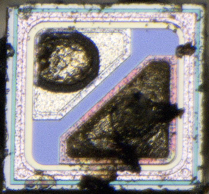
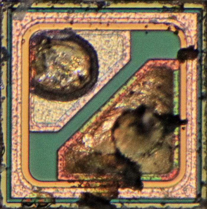
The edge length of the die is 0,32mm. The design can also be found in the PNP transistor BC560C (
https://www.richis-lab.de/Bipolar52.htm). The NPN transistor BC548C (
https://www.richis-lab.de/BipolarA15.htm) contains these structures too, but the outer metal frame has been omitted.
https://www.richis-lab.de/BipolarA18.htm
...
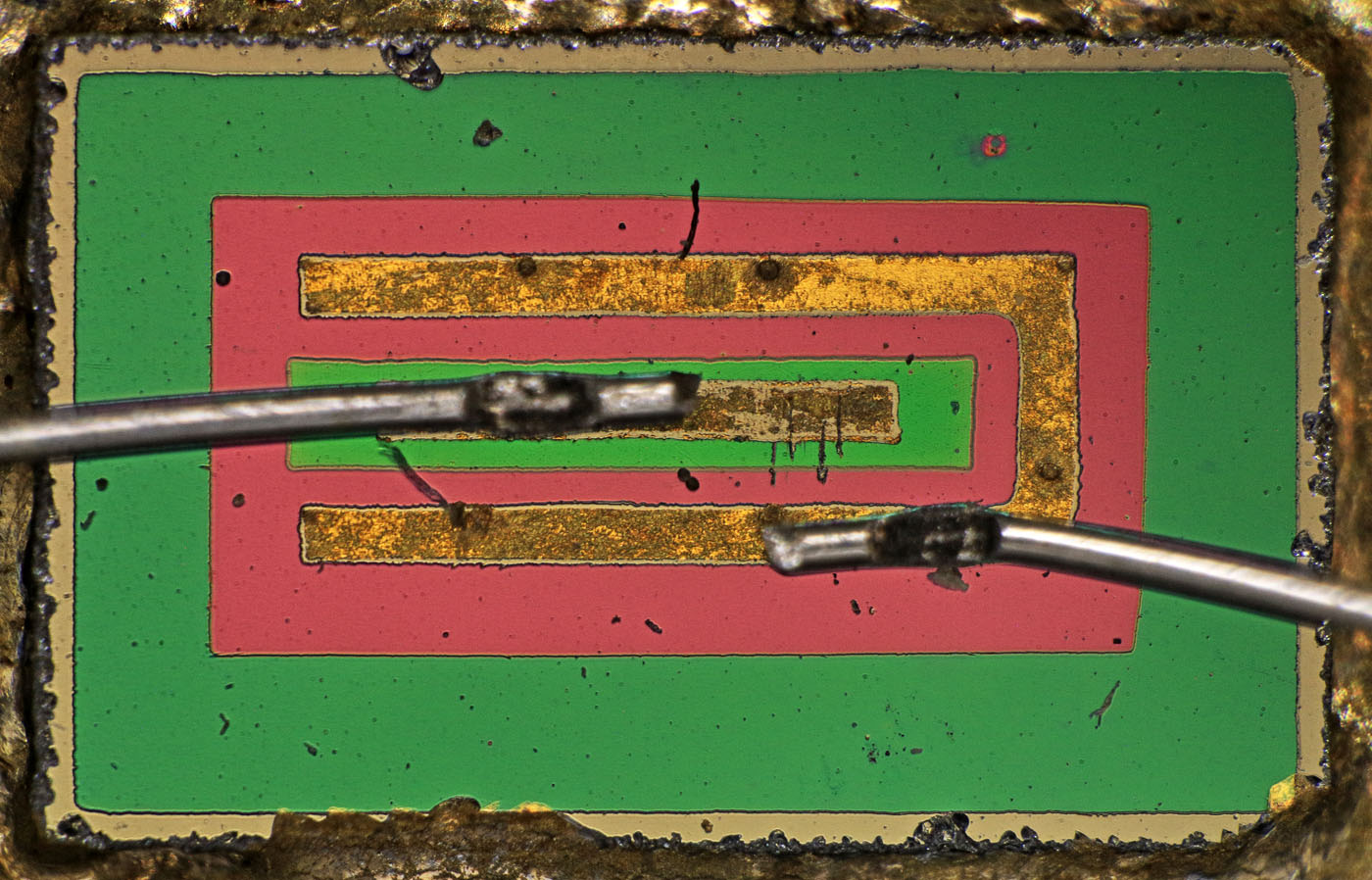
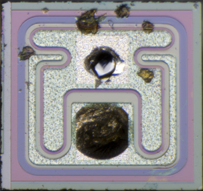
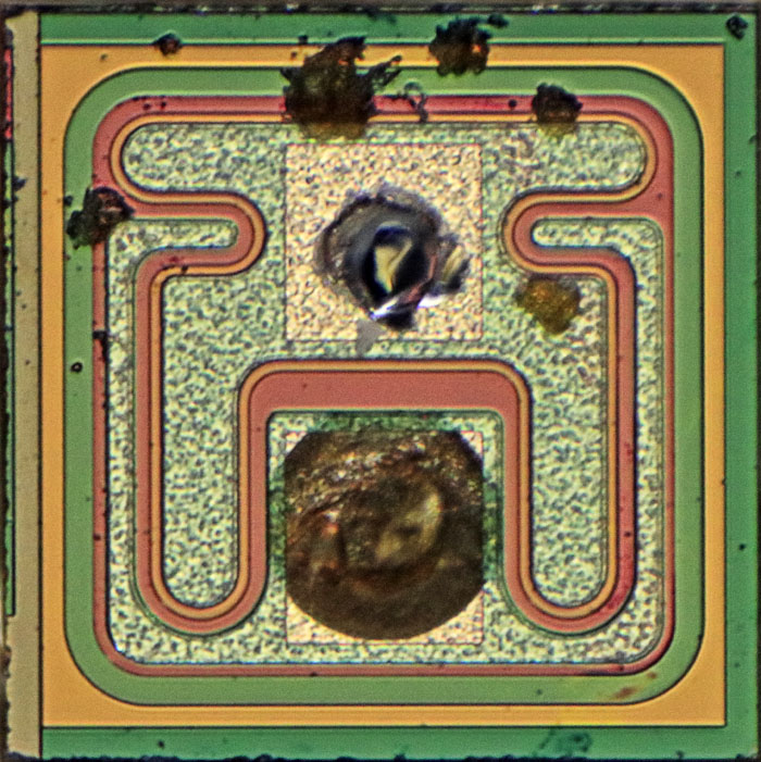
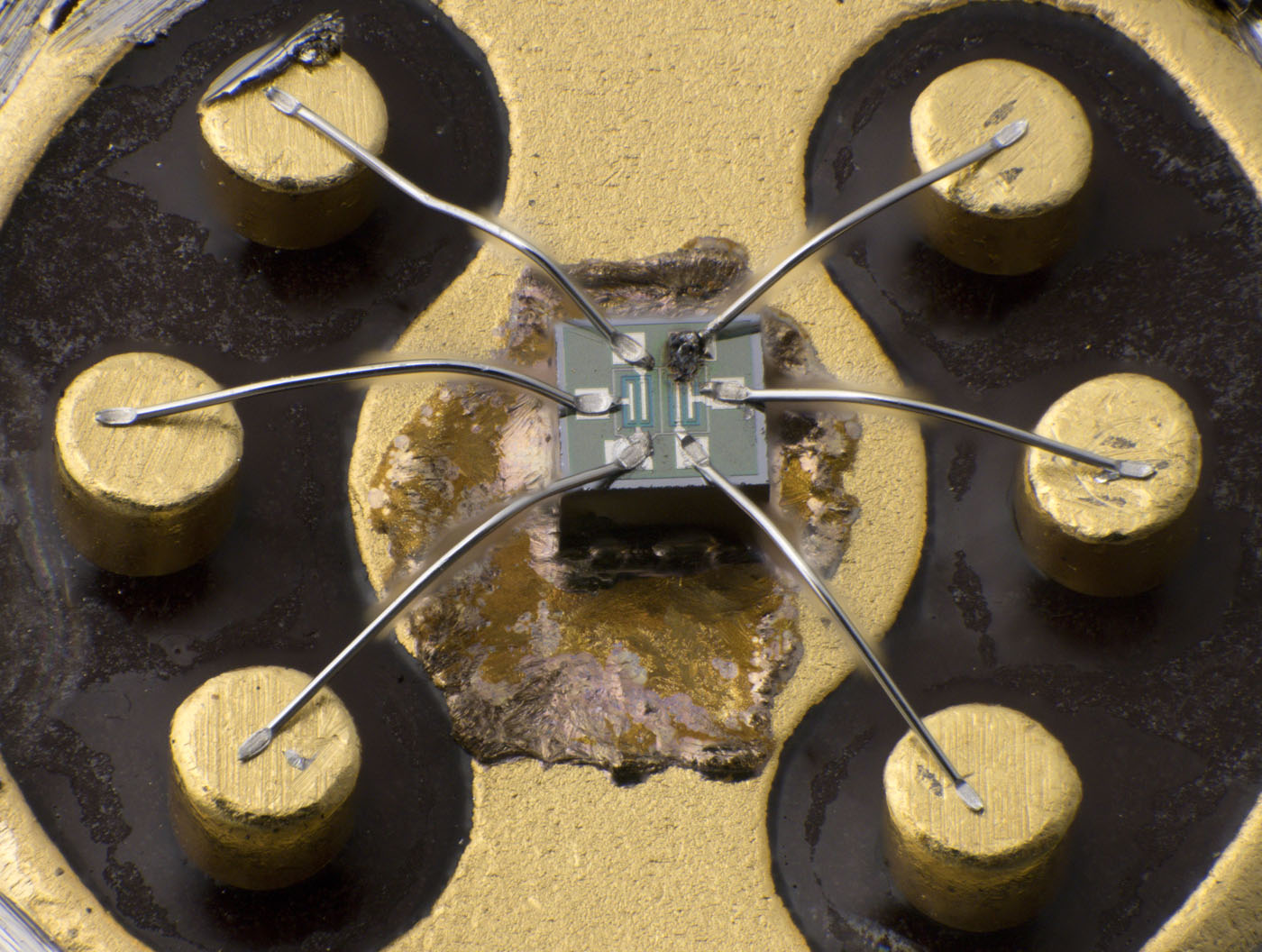
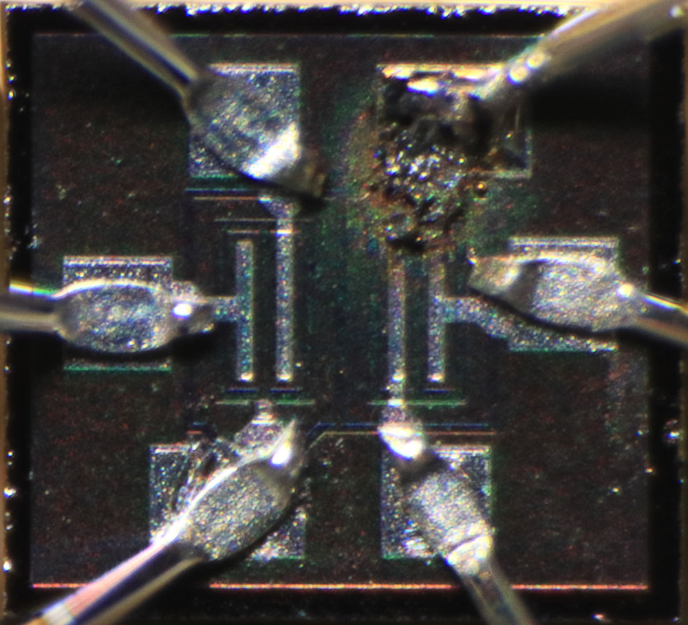
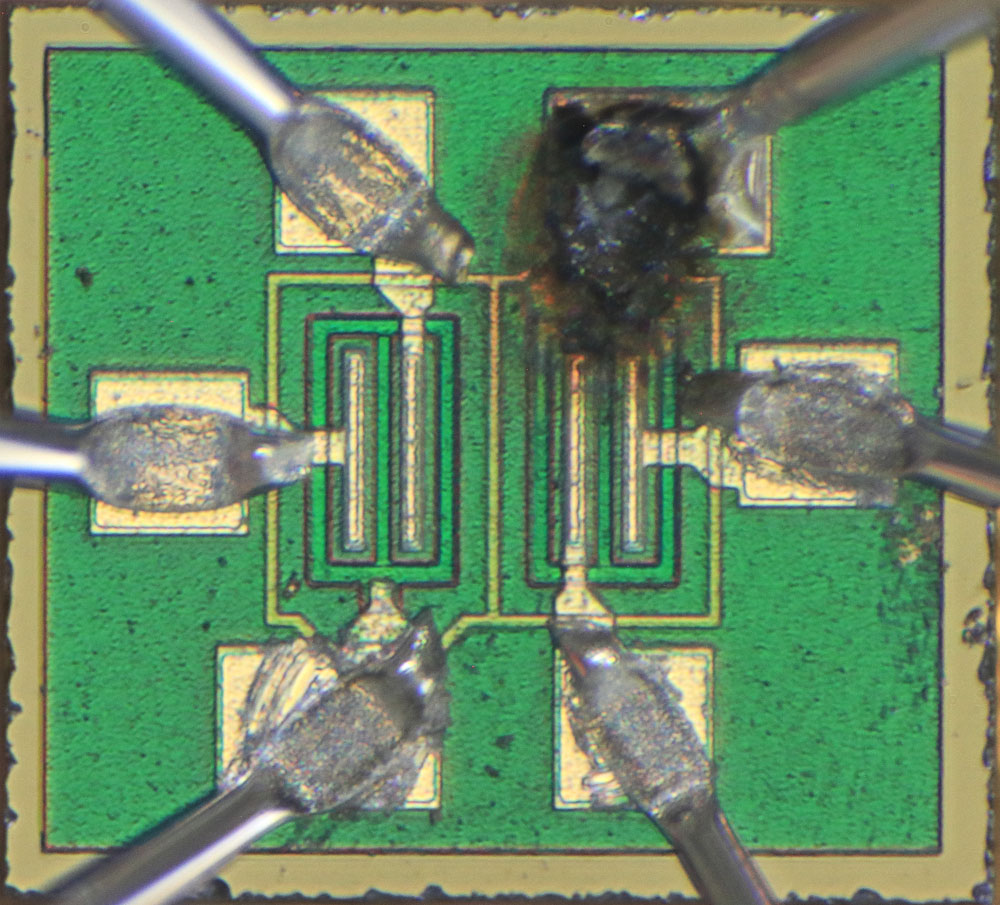
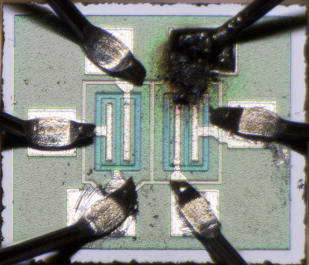
I took some IR pictures of the HFO SL113, this old HF silicon transistor:
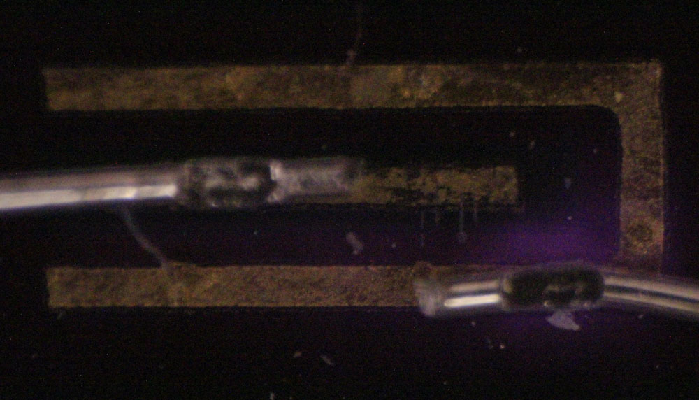
In this image a current flows across the base-emitter junction with the collector open. As described with the SF137 (
https://www.richis-lab.de/Bipolar75.htm#IR), some light occurs at the base-collector junction. The light is very non-uniform. The upper area remains dark and in the lower area, especially the area under the bondwire is illuminated.
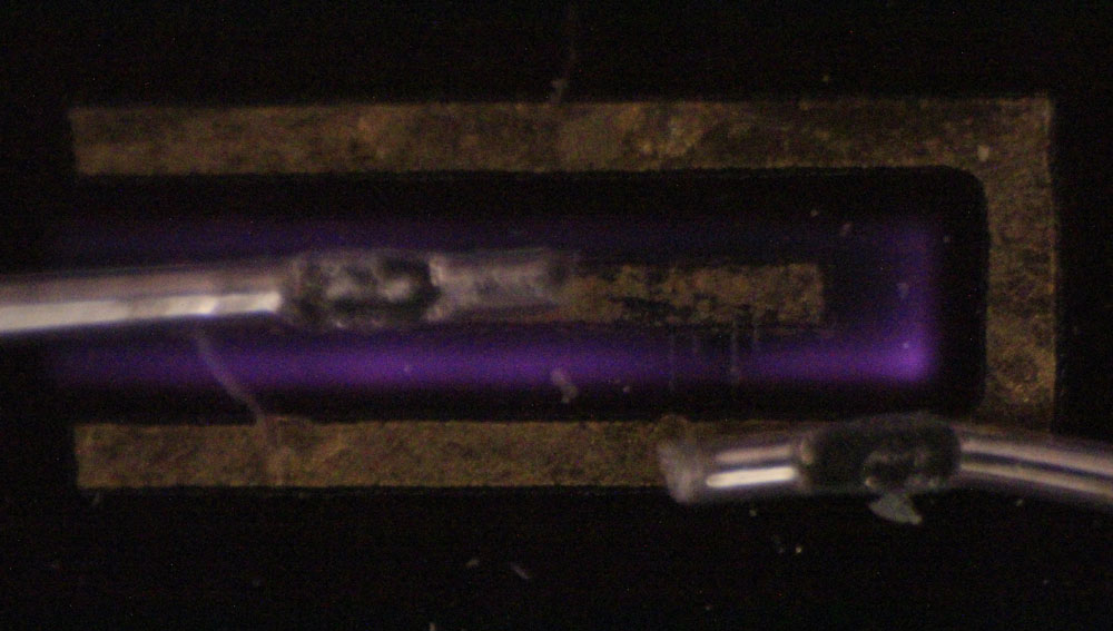
As soon as there is a current flowing through the collector, the light shifts to the emitter area. The light there is somewhat more homogeneous, but still clearly more irregular than for example in the 2N389 (
https://www.richis-lab.de/BipolarA09.htm#IR).
The images suggest that either the structures were fabricated irregularly or the areas have such a high resistance that there is no homogeneous current distribution. Since this is a very early silicon power transistor, such deficiencies are hardly surprising.
https://www.richis-lab.de/Bipolar29.htm#IR
Hello,
Very interesting discussion.
By any chance, do you have some pictures of the NS LM194/394 ??
If no, could you provide these pictures ?
Thanks in advance.
Alain.
I have to take a look into my warehouse, if there is a LM194. If not I can source one.
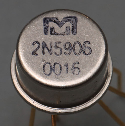
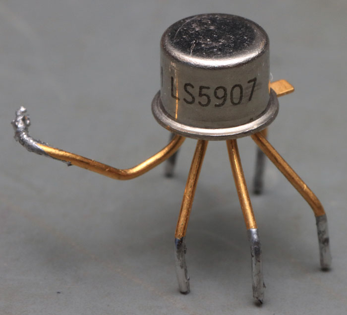
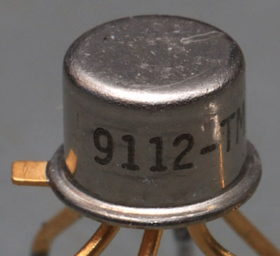
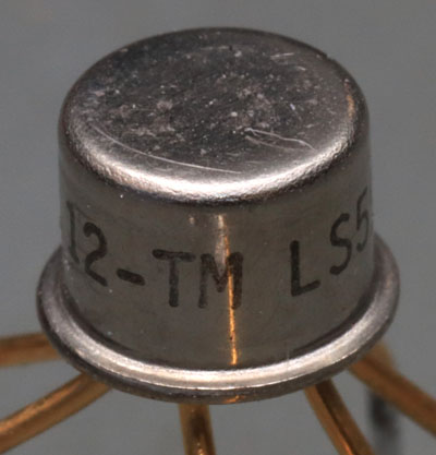
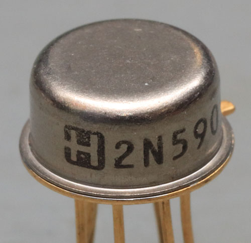
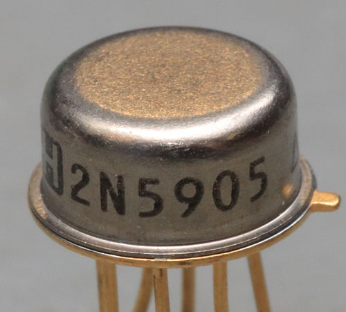
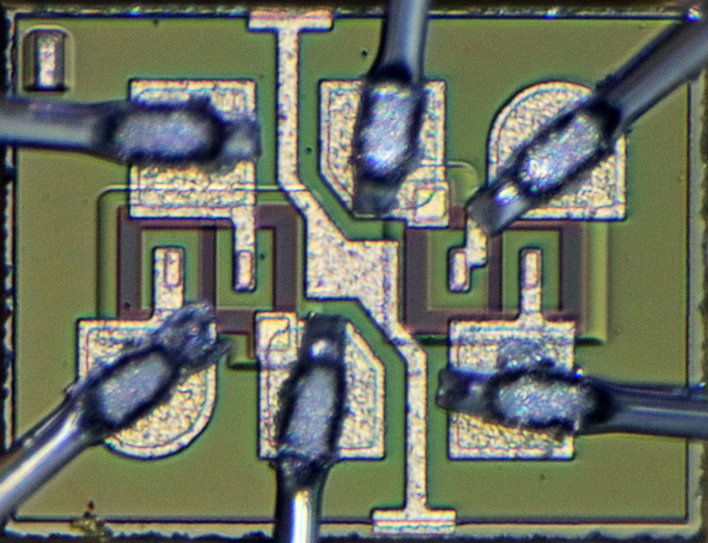
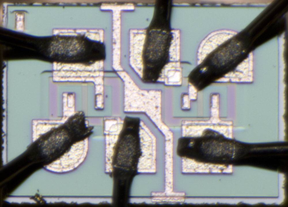
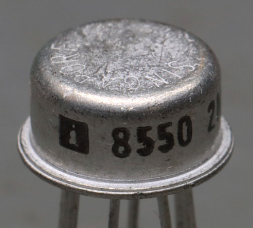
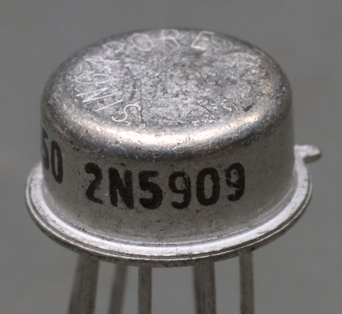
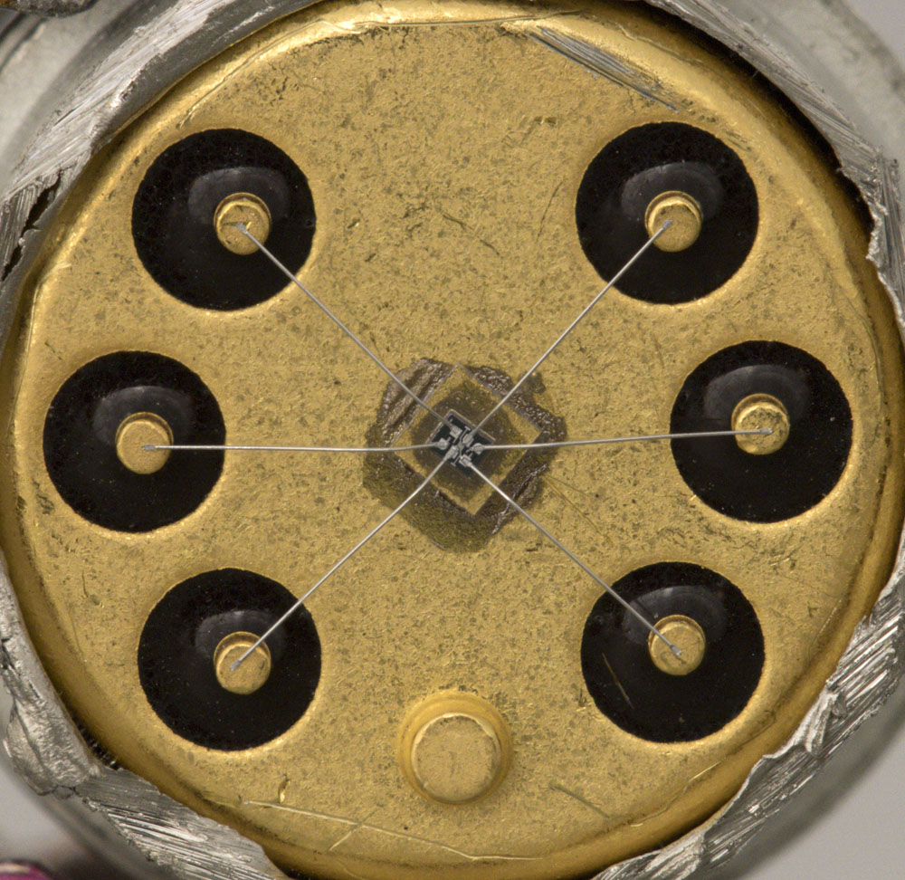
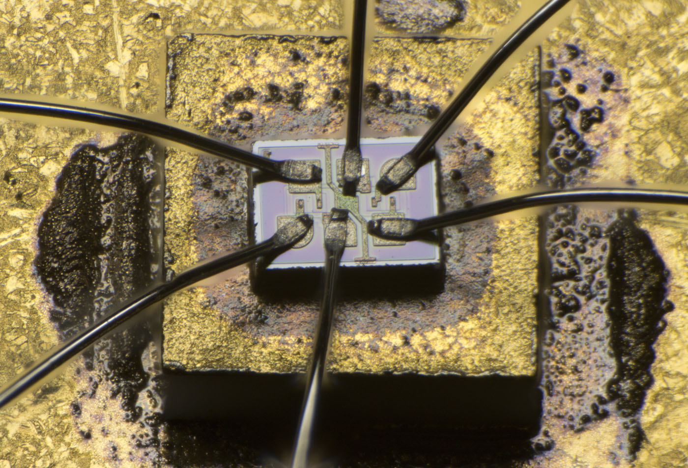
Does anybody know this logo? It looks like Micro Power Systems. They sold variants of the 2N590x under the names MP590x but their M is different.
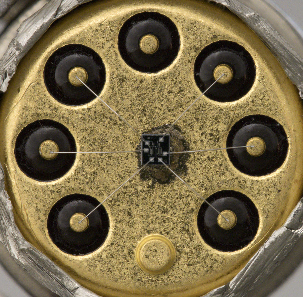
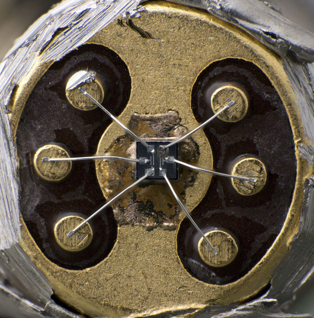
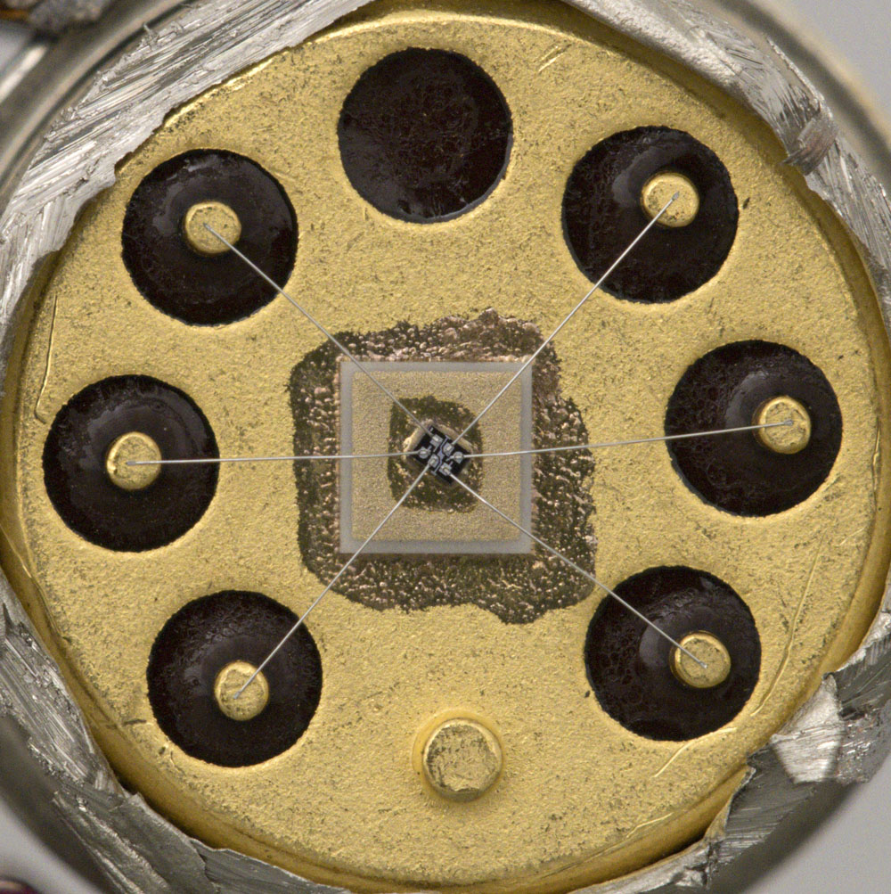
Unlike the 2N590x variants from Intersil and Harris Semiconductor the die here is not isolated from the package.
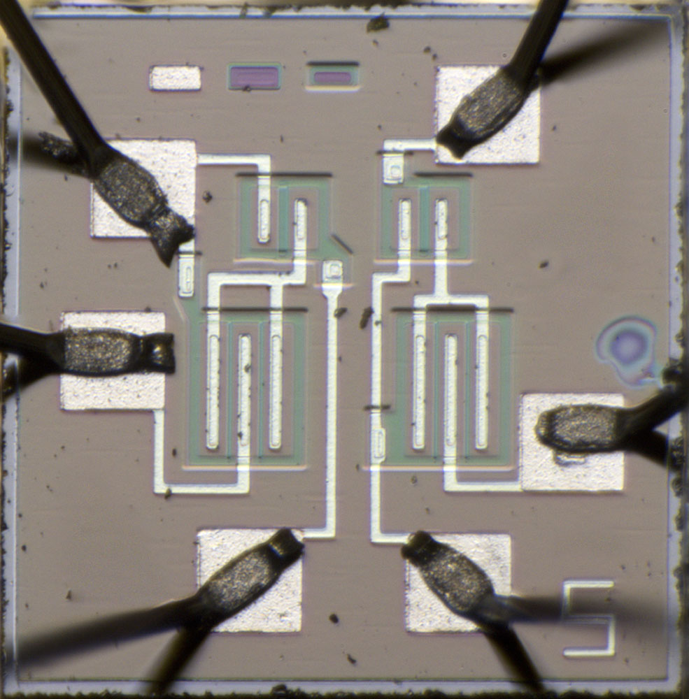
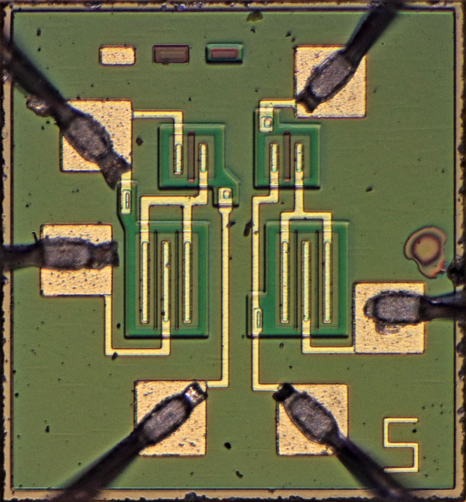
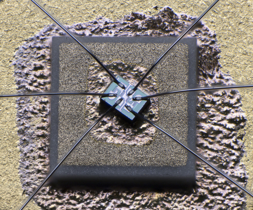
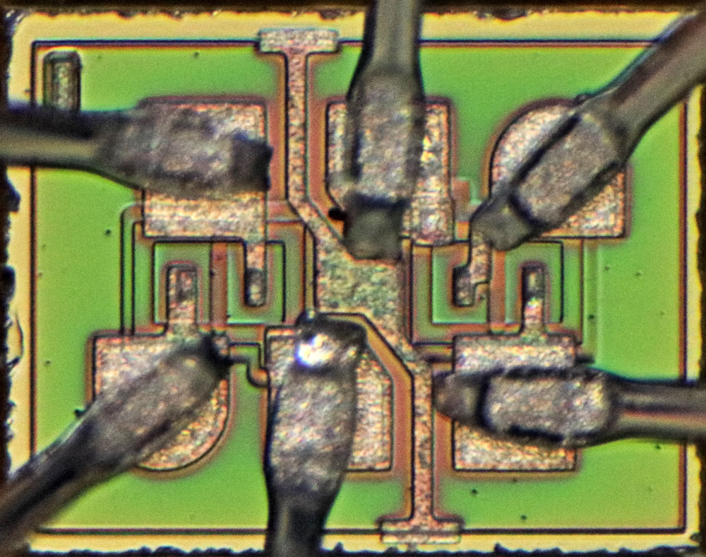
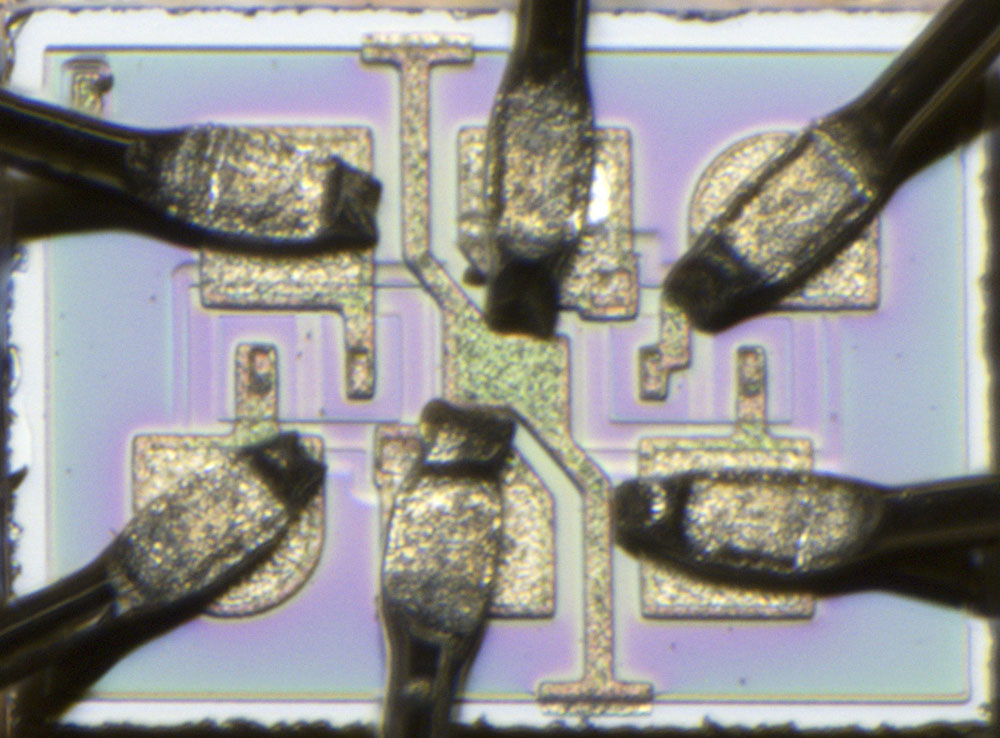
The dimensions of the dies are 0,72mm x 0,66mm. Structures for monitoring the manufacturing process are integrated at the upper edge. The character in the lower right corner, a S or a 5, does not allow us to draw a conclusion about the manufacturer.
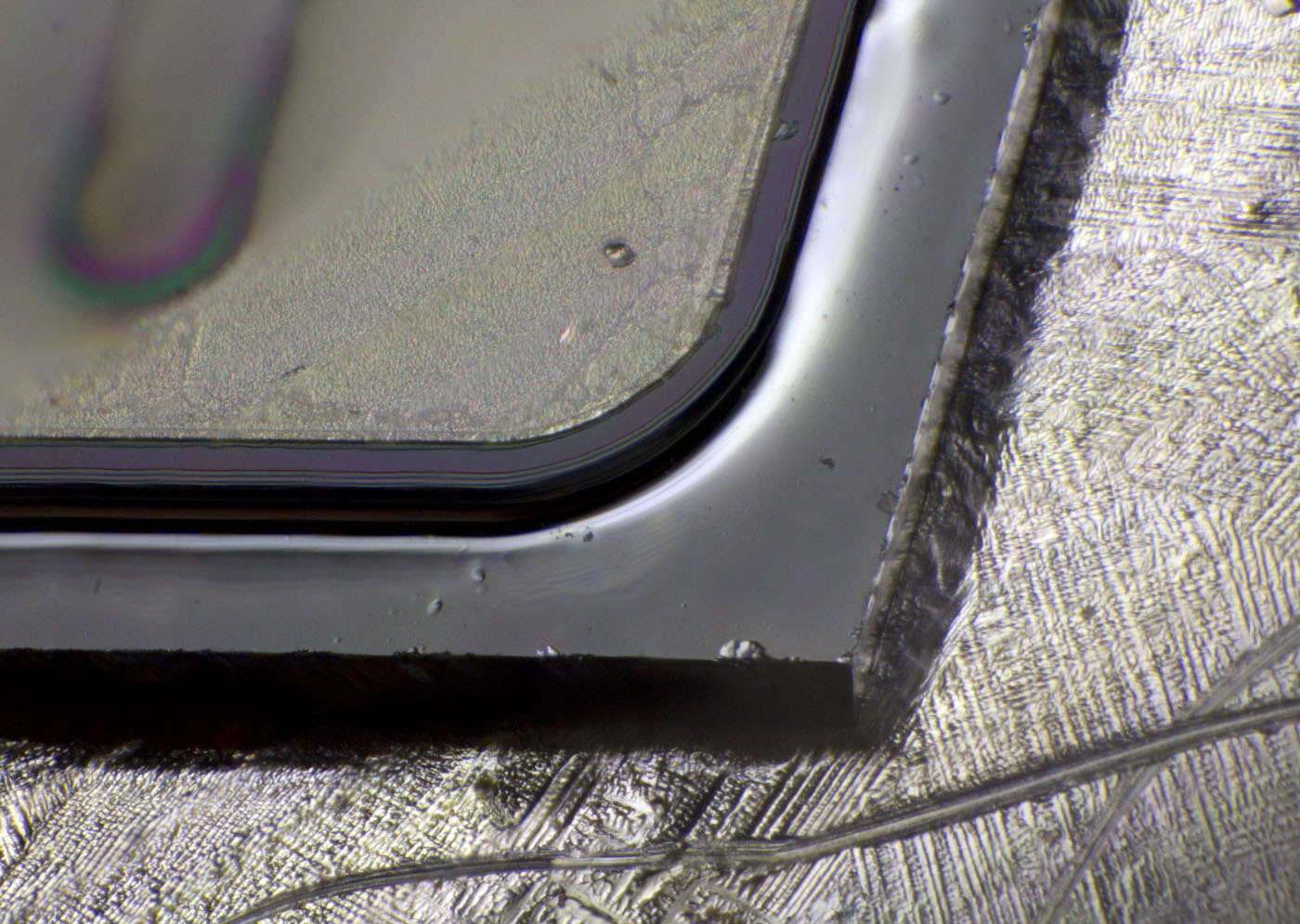
An interesting artifact can be found at the right edge. Here, the passivation seems to have delaminated in a small area due to a damage on the edge.
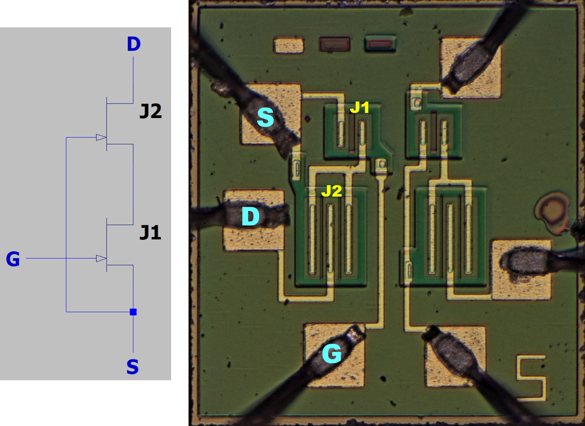
It is immediately noticeable that this are not just two JFETs. Two cascode circuits have been integrated here. The small JFET J1 is the input transistor, while the larger JFET J2 shields the input transistor against the output. This reduces the effective gate drain capacitance.
The gate electrode of J1 is not only shorter, it is also thicker than the gate electrodes of J2. The different geometries are advantageous for the operation of the cascode circuit, in which the upper JFET operates in the linear region while the lower JFET operates in the saturation region.
https://www.richis-lab.de/FET29.htm
I have some pics of various 2N2222 transistors produced by different manufacturers.
Here’s the Motorola transistor.
MOTOROLA JAN 2N2222A


CRP INDUSTRIES JAN 2N2222A