-
I just took patz' sources to turn my Tekway DST1062 into a DST1202.
nice job!
as mentioned at the beginning of this thread for manual hack you need to change not only the- After I changed the bandwidth, TTScope identifies the scope with the new bandwidth, and I may switch to 2ns timebase, but the scopes system information still reads dst1062b.
Is this the suspected behaviour?
/dstxxxx file (which is responsible for the bw filter and model based then for enabled features)
but also the logotype/logotype.dis files (and to sys.inf /tmpdst, however they will be recreated at boot time properly
in case they wrong). The logotype/logotype.dis files are not only responsible for "boot logo" but also for device
name (the displayed in system info). So in principle you can have higher bw (because you renamed /dstxxx file)
and old logo and old dso name (because you not changed logotype+.dis)- Unfortunately I don't have a adequate source to check the actual bandwidth, thus I just "listened" to some USB communication to get an idea of it (poor thing, I know).
The rise-time improvement was from 5,7ns to 4ns (3.7 at best, 61MHz -> 95Mhz)
Now I'm considering my probes.
Pinsonne offers three different accessories probes. One for each bandwidth, but they all seem to be identical.
Of courxe I have only the 60MHz version.
http://www.pinsonne-elektronik.de/pi10/pd111.html
http://www.pinsonne-elektronik.de/pi10/pd108.html
http://www.pinsonne-elektronik.de/pi10/pd107.html
Do you have any experience, which bandwidth you could reach with the original probes?
they made by Texas whatsoever probe company (china of course). They not that bad, i'm using 250MHz probes from them daily
and happy with the freq response.
The org. 60MHz probe is good up to 85-90MHz from what i remember, these probes on third link (200MHz) are good replacement.
Sure, they looks all the same, but there is definitely difference in bw.
Actually many ppl doing hacking these DSOs without thinking about probes, in principle sometimes (based on shop/price)
it is cheaper to buy 100MHz model with 100MHz probes (and they good up to 130-150MHz or so) instead of 60MHz
with 60 MHz probes - you will still need something about 100-200Mhz for daily work and maybe a good set of 500Mhz
passive or active probes.- How did you test your improvements?
Did you take the original probes or something different?
simple by using every day And no, i'm unsing as said above 250MHz Texas passive probes for default tasks
and 500MHz active probes for RF tasks.
When i change something in the firmware the i use of course a set of equipment to check the changes,
something like rise time with fast pulse generator. - After I changed the bandwidth, TTScope identifies the scope with the new bandwidth, and I may switch to 2ns timebase, but the scopes system information still reads dst1062b.
-
@Tinhead, how did you manage to reverse engineer the schematics? Looks like a very difficult task, did you have to depopulate the board first? Or did you use a buzzbox method? What tools are used? Is it possible to leave the board populated and achieve good results?
Thank you -
@Tinhead, how did you manage to reverse engineer the schematics? Looks like a very difficult task,
well it is dificult, but everything is just question of time and/or knowledge.did you have to depopulate the board first?
Typically it this depends on tool you have, the actual PCB and the reason why you doing reversing.
In case of the DSO i unpopulated few things to validate my boundary scan results or
to reduce the chance of an error (with cont. checker/buzzbox you can get wrong values sometimes),
later as i was ready with raw schematics i unpopulated most passive parts to make the schematics really complette.Or did you use a buzzbox method?
sure, when possible or no other way availableWhat tools are used?
Continuity checker - it must be always a good one (low voltage!!!). Everything below 0.7V is ok,
i'm using one with 0.4V capable of driving 0.5mA max.
Boundary scan software (evt. hardware too) - there are few good tools,
however i'm using Universal Scan from Ricreations ( http://www.universalscan.com/) .
It is not that expensive (850$ only, if you compare to other products you will see it is cheap!).
I remember the trial version was working without any restrictions, so you might use this as well for 30days?
The hardware you need to use Universal Scan -Y For all kind of (mostly ARM, it works e.g. with memories too)
chips Amontec JtagKey or Key2 (original, clone will not work with Universal Scan!), for FPGAs/CPLDs the specific
one form Xilinx or Altera (well or Digilent).
JTAG/Debugger tools - i have a complette set : Ulink V2 and Pro (which i got with MDK), H-JTAG Pro USB (i love it, much better
than the crap J-Link from Segger and their crap j-flash software), Amontec JTAGKey and Key2, Renesas FoUSB/R8a, Cypress
IceCube/MiniProg1/3, MSP430FET, STM ST-Link1/2 (actually from STM dev boards but STM is having anyways cheap tools),
Xilinx/Actel/ALTERA JTAG cables (clones only), Atmel JTAGs (ICE MKII clone, ICE3 ordered), OpenJTAG (from 100ask.net),
puhh did i miss one? probably. You don't need of course so many tool, however it is very handy to have a way to
program/debug or scan a chip. For the DSO i've used for boundary scan only Altera JTAG cable and Amontec JTAGKey2.
For NAND and testing of some S3C2440 SoC features H-Jtag Pro USB. For sure you might ask now for what reason
i need ISP/Debugging tolls, well it might be sometimes easier to code something to simulate a situation to get some results
from a chip attached to known chip (you can't just connect 32 port generators, 64 port LA without getting crazy, a few line
in code are easier and tracable!).
Stereo Microscope - sure you can work without but it is easier to have it.
DMM, DSO, Signal Generator and even sometimes Spectrum Analyzer.
Datasheets, bsdl files (in case you use boundary scan, believe me once you understood what they
doing and how they working you will never ever wish to work without)
When you decide to unpopulate parts then of course proper tools like good IR Reworkstation
(it can be cheap china thing, but you probably will have to modify a bit), set of small universal stencils,
reballing tolls, ChipQuick SMD1 (a lot of that!!) , tons of IPA (Isopropyl alcohol), Kimtech kimwipes (they are just the best)
well the typical things.Is it possible to leave the board populated and achieve good results?
sure, with proper tools no doubt. Even with enough time (mostly for studing datasheets!!!) and only continuity checker
you might achieve very good results. However sometimes you will have at least to unsolder one or more pins
(to disable in hard way a chip). For all kind of passive components you will have for sure unpopulate them to get
exact values (analog part definitely, digital not necessary - datasheet/app note are mostly what exact enough).
-
Hi,
I've been following this thread for some time. You guys are the best!
So, I finally have a question of my own. Hope this is the right place for it.
Would it be possible to put a custom boot screen in place of the default?
You know when you turn it on it has "the Screen" that shows brand and model.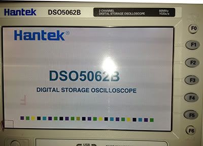
-
I encountered (probably) the same problem as djeans and paul described on the last pages.
DSO5102B, no hacks, 2.06.3(111226.1).
I updated the firmware today for the first time ever on this unit. It locked up a few minutes after the update while in splitscreen and changing the memory depth. After reboot it showed the splitscreen and even after each reboot the updated date and time. but no reaction to any key pressed and no signal shown.
I tryed to press "default setup" while booting (hitting the key as often as possible) and after 5 or 6 reboots without effect it now responds again.
Maybe i'll try the fw posted by tinhead (ps thanks for all the work)
<edit>
updated to 120112.1. problem presists. trying to change mem depth from 4k to 40k results in locked unit...
<edit 2>
maybe it was just luck the first time where pressing "default setup" helps or i did something other i don't remember. Now it doesn't help. So I'm waiting for the usb <> serial ttl connector to arrive
original fw, bugs but never encountered this "permanent freezing". after reboot all was ok again.
model dso5102b
softversion 2.06.2(101028.0)
hard version 0x555583e8
after (first) update today
model dso5102b
softversion 2.06.3(111226.1)
hard version 0x555583e8
-
So, I finally have a question of my own. Hope this is the right place for it.
Would it be possible to put a custom boot screen in place of the default?
You know when you turn it on it has "the Screen" that shows brand and model.
sure, just build your own logos and replace the coresponding files in /logo directory on DSO
On Hantek their like:
hantek_DSO5062B_down.ico
hantek_DSO5062B_mid.ico
hantek_DSO5062B_up.ico
hantek_DSO5062C_down.ico
hantek_DSO5062C_mid.ico
hantek_DSO5062C_up.ico
hantek_DSO5102B_down.ico
hantek_DSO5102B_mid.ico
hantek_DSO5102B_up.ico
hantek_DSO5102M_down.ico
hantek_DSO5102M_mid.ico
hantek_DSO5102M_up.ico
hantek_DSO5202B_down.ico
hantek_DSO5202B_mid.ico
hantek_DSO5202B_up.ico
hantek_DSO5202M_down.ico
hantek_DSO5202M_mid.ico
hantek_DSO5202M_up.ico
where *_xxx is for the logo location during boot (yes, there are 3 pictures, Hantek logo, name in the middle and these
colored bar on bottom - down)
On Tekway the are named bit different:
dst1062b.ico
dst1102b.ico
dst1202b.ico
dst3022b.ico
dst3042b.ico
dst4042b.ico
dst4062b.ico
dst4102b.ico
tekway.ico
website.ico
Format of tese files (they not icon files, only named like that) is something raw 16 or 8 bit RGB,
i did played a time ago with that, don't remember exactly the values now.
-
Thanks tinhead! I had no idea those were separate images. Just figured it was a single image...Quote
sure, just build your own logos and replace the corresponding files in /logo directory on DSO
And those are accessed via Uart only. Right?QuoteFormat of these files (they not icon files, only named like that) is something raw 16 or 8 bit RGB,
i did played a time ago with that, don't remember exactly the values now.
Ok so, I know you say you don't remember exactly. And i appreciate everything thus far.
Just one more question to possibly help me to this end.
There not Icon files but there labeled .ico. "Ok no problem"
So then I'm guessing I could make them in say, "photoshop" and try saving them as .bmp's with varying bit depths then changing the suffix from .bmp to .ico until I find the proper bit depth that works?
-
well, create bmp and convert it with tool like Img2Lcd.exe to bin. There are many tools like that,
good starting point is to search for "FriendlyARM S3C2440 boot logo tools"
http://code.google.com/p/ab-embedded/downloads/detail?name=Image2Lcd%2BV3.2.rar&can=2&q= -
Perfect, I'll give that a shot Thank you
-
I'm reading this thread since beginning and i eventually decided to join the forum. I'm about to purchase a new oscilloscope which i will use mainly for power electronics debug, power supplies, inverters, AC drives. I would like to ask your opinion regarding the choice. Among the candidates are the DSO5102B, Rigol new series, DS4024 or Tek DSO/MSO4024. I know that the last two might be overkill, also their price is at least 5 times higher, but i might use the scope in the future to debug digital designs as well as analog and power designs.
Is there any way that either TEKTRONIX DPO/MSO2024 or Rigol DS4024 100MHz versions could be "upgraded" to 200MHz similar as the current Tekeway ? I search on internet without any relevant result.
Thank you. -
Hello again,
Thank you for all your help thus far.
Ok I'd say I have a pretty good/basic grasp on the linux commands required to navi/edit in PuTTY via usb-TTL adapter (Been late night Cramming Like the days of Ole')
So I'm still playing with the custom logo's, right.
Reading everything I can find but I'm having problems in one area particularly.
I feel down right "DUMB" for having to ask such a noob question and it is probably stupid easy and I'm just over looking it but,
How do I transfer the logo files from the oscilloscope to my Pc or the other way around, my newly created logos from the pc to the oscilloscope.
-
Hello again,
Thank you for all your help thus far.
Ok I'd say I have a pretty good/basic grasp on the linux commands required to navi/edit in PuTTY via usb-TTL adapter (Been late night Cramming Like the days of Ole')
So I'm still playing with the custom logo's, right.
Reading everything I can find but I'm having problems in one area particularly.
I feel down right "DUMB" for having to ask such a noob question and it is probably stupid easy and I'm just over looking it but,
How do I transfer the logo files from the oscilloscope to my Pc or the other way around, my newly created logos from the pc to the oscilloscope.
hehe ... simple thing. In principle when you connect with putty to the linux shell of the DSO you can access to the
file system. The logo files are in /logos directory, a USB flash drive (yes , exact this way to go!!!) will be automounted when you instert it to /mnt directory. So then in prnciple insert usb flash drie and do cp /logo/* /mnt and you have them, and of course vice
versa after you changed them on your PC. To ensure they not get damaged do once "sync" and umount /mnt before you remove
the usb flash drive ...
-
ahh yes!
I had not thought of that. thanks again!!! -
LOL
why that? well .. nice story ... a guy in Germany was about to save some money, so he decided to
buy from Conrad.de a VOLTCRAFT DSO-3062C instead Hantek or Tekway from another seller.
As he is a beginner he said "200EUR is a difference, so i decided to buy the cheaper and slower model"
Note - this Voltcraft is actually nothing else that Hantek (or Tekway) clone, 60MHz scope with 500MSs.
When you look on Hantek website you will find such scopes - Hantek DSO5062C, or from Tekway as DST4062B.
I even posted on the begin of this thread "don't buy these DSOs, they different!!"
However, 200EUR is lot of money, so he take the risk and bought it ...
He made some pictures and guess what?! It is 1GSs DSO and not 500MSs!!!
This means Hantek/Tekway (well Voltcraft somehow too, they probably even don't know what they selling)
are simple too lazy, they not only selling exact equal PCBs/DSOs marked as with different bandwidth but
even as "with different sample rate" (be careful, Tekway is having DST3000B - they really slower!!
i have pictures showing totaly different PCB).
So for 299EUR this guy got a beautiful 1GSs HanTekway (with stupid Voltcraft logo, but yeah, this can be changed)
with frontpanel tagged as 500MSs 60MHz (who cares about the frontpanel sticker ...)
And of course this scope is 100% hackable, so he got for totaly 299EUR a DSO with 200MHz bandwidth and 1GSs sample rate ...
isnt' that cool? I think it is!
So when you need a Hantek/Tekway DSO buy such Voltcraft asap, no idea how long Conrad will have them in stock
http://www.conrad.de/ce/de/product/122464
Btw, the tool from McCurrent wrk also for Voltcraft models
https://www.eevblog.com/forum/general-chat/hantek-tekway-dso-hack-get-200mhz-bw-for-free/msg91877/#msg91877
-
What a great morning over here in Germany!!!


Guess what, I was looking for such a scope since a few weeks and of course I quickly ordered one! So first of all thank you for this info!
Ironicly Conrad is known to be quite expensive.
One thing I realized on the Conrad page:
As they say it is a 500MS/s scope, wouldn't that mean this stupid equivalent sample rate would be halved, too? But it still says 25GS/s.
Just one question:
"Is" it the 1GS/s version, or do I need to hack it to be 1GS/s? How do I proof or measure this? Were do I have to hook up my LA for timing measurment?
-
One thing I realized on the Conrad page:
it is physicaly 1GSs device, it does have the same PCB, same amount of ADCs, actually everything is the same as for
As they say it is a 500MS/s scope, wouldn't that mean this stupid equivalent sample rate would be halved, too? But it still says 25GS/s.
example on DSO5062B.Just one question:
"Is" it the 1GS/s version, or do I need to hack it to be 1GS/s? How do I proof or measure this? Were do I have to hook up my LA for timing measurment?
as said above, no need to hack to 1GSs, it is 1GSs scope out of the box!
When you go to Utility, page2/3 and click on Sys Status
you will see some actual DSO parameters. One of them is the actual sample rate. On these scopes if set
to 4k sample memory, one channel enabled and with timebase 8ns/DIV, 4ns/DIV and 2ns/DIV you will see
there 1GSs. Conrad probably even don't know what they selling. -
Thanks for the info Tinhead!
I just ordered this scope from Conrad. I think the only other german store that sells this scope is Pinsonne Elektronik (http://goo.gl/1EViS), and the scope is around 200 Euros more expensive there. Hope I get the right version though.
Any way to identify it's the right model/hardware?
Gruß,
Florian -
Any way to identify it's the right model/hardware?
if it works you got the right device
But honestly, don't worry, ppl from austria and holland confirmed to me that
Conrad is having "proper" hardware everywhere. Sure, it might happens that due presure from other
distributors* HanTekway will change these 500MSs to what they should be - 500MSs, but this will
not happen that fast (and even if, in EU you can always send back to Conrad).
*- why other distris are pissed off? well maybe a bit because i made it public, but honestly when not i someone
else would do it anyway. The point is, Hantek/Tekway decided to save production costs by producing
of single PCB for multiple models. In principle not big deal, even when ppl hacking "B" models to 200MHz bandwidth,
(i always said "be fair, buy 100MHz model, these few bucks are important for manufactrer and you getting
probes for free - because when you hack you still need some probes") everybody could be happy.
Even the ebay "gray market" competitors are not that tragic - ppl who smart knows that "if" something get broken it's better
to have someone near you. And don't forget - not everybody is hacking!
But with these Voltcraft models (or well, Hantek "C/N" models) the situation is totaly different.
They costs 299EUR, that 400USD. Now imagine when you buy DST1062B from Tekway directly (not a single but 20+pcs)
you have to pay per unit 380USD (Hantek DSO5062B about 340USD - so lets take avg. 360USD/pcs - and yeah, that's my price,
it might varry a bit depending on who is buying and how much, but i think this is a good example price).
Now you have to pay of course shippment, no matter if 1 or 50 it still costs per kg. Even with good condition
you have to add at least 50-80USD per unit (makes at least 410USD total). Now in EU you have to pay VAT,
avarage is 20% i think?, that's 492USD total. And now compare to these Voltcraft DSOs, they IDENTICAL and
92USD cheaper!! So how the hell can distributor import and sell original 1GSs models now? No way!
Now when you buy from Conrad 10+pcs you will get them for 275EUR (or 369USD) each! - with warranty and local VAT.
123USD cheaper than imported from manufacturer (and the distributor did not made single $ win!!!) That's crazy.
And note, i'm not talking about hack!!! Out of the box the unit Conrad is selling is having exact the same
specs like Hantek DSO5062B or Tekway DST1062B - 60MHz bandwidth and 1GSs (instead of like printed out 500MSs) -
and that's the real issue!!!
So if you wish one, buy fast. I don't think that this will be ignored by both manufacturers, maybe Conrad price will rise
up, maybe price for original 1GSs models will get reduced, maybe both manufacturers will produce real 500MSs models,
we will see. -
Quote
well, create bmp and convert it with tool like Img2Lcd.exe to bin. There are many tools like that,
"
good starting point is to search for "FriendlyARM S3C2440 boot logo tools
Ok I have try using img2lcd to convert .bmp to .bin then changing the suffix to .ico but to no avail. none of them seem to work. it has so many different options and all the help files are in Chinese (I can't read Chinese) Do you know what setting to use.
Some of the options are
256 Color-------------RGB332 Palette, Grey Palette
4096 Color-------------12bits(continue Bits), 16bits (WORD)
16-bit Color-------------(R:5bits,G:6bites,B:5bits), (R:5bits,G:5bites,B:5bits)
18-bit Color-------------6Bits in Low Byte, 6Bits in High Byte
24-bit Color-------------
32-bit Color-------------
Output Options
Output file type: .bin .c .bmp and more
scan modes: several different kinds
BitsPixel: monochrome, 4 color, 16color, 256 Color, 4096, 16-bit TrueColor, 24-bit TrueColor, 32-bit TrueColor
Max width ans height.
check boxes Include head data, Scan Right to Left, Scan Bottom to Top, MSB First.
Any thoughts....
I have also Tried searching "FriendlyARM S3C2440 boot logo tools" But there are none that have anything to do with these .ico files.
All i could find were things about recompiling the kernel.
I'm totally suck. IS there anyway at all to open the the default logo files to get an idea of file heights and widths etc....
Thank you IF you have any ides that would be awesome!
Sobiguy
-
A quick look into a .ico file tells me it is rather primitive. It starts with two 32 bit numbers, giving width and heigh (or hight and width) of the image in pixels. Then follows what looks like 1 byte per pixel data, indexing into a colour pallet. The colour pallet, however, is not part of the file. It is likely hardcoded in the software that reads the file.
-
Nice detail in Conrad:
1062C 60MHz in text but in picture front panel read 100MHz (and this 500MSa/s and oh yes also it is exactly true. It is 500MSa/s maximum! If it is used with 2 channel so, there is not anything exactly wrong, also becouse 60MHz model real -3dB point is around or just over 100MHz.(without any mod ) :
-
A quick look into a .ico file tells me it is rather primitive. It starts with two 32 bit numbers, giving width and heigh (or hight and width) of the image in pixels. Then follows what looks like 1 byte per pixel data, indexing into a colour pallet. The colour pallet, however, is not part of the file. It is likely hardcoded in the software that reads the file.
How are you looking at it! if I open it in notepad or somthing like that all I get is "Goble-de-gook"<---technical term<
Can you pick one and possibly give an example. So if it's pretty primitive what do i have to do to edit/make one? -
Nice detail in Conrad:
1062C 60MHz in text but in picture front panel read 100MHz (and this 500MSa/s and oh yes also it is exactly true. It is 500MSa/s maximum! If it is used with 2 channel so, there is not anything exactly wrong, also becouse 60MHz model real -3dB point is around or just over 100MHz.(without any mod ) :
but you know that this is bullshit - typical what you will see on enclosure is the max max max value
I got firmware back from such Conrad DSO - 100% 1GSs Hantek model, even better - it was originaly DSO5202B ...
-
Nice detail in Conrad:
1062C 60MHz in text but in picture front panel read 100MHz (and this 500MSa/s and oh yes also it is exactly true. It is 500MSa/s maximum! If it is used with 2 channel so, there is not anything exactly wrong, also becouse 60MHz model real -3dB point is around or just over 100MHz.(without any mod ) :
but you know that this is bullshit - typical what you will see on enclosure is the max max max value
I got firmware back from such Conrad DSO - 100% 1GSs Hantek model, even better - it was originaly DSO5202B ...
Yes I know... of course.
You mean that also HW is with 5202B components related to BW.
If this all, meybe Conrad have busy days for ship all purchased 3062C's
I do not know what is shipping price for other countries.
(maybe they close this offer soon..... ) -
It is marked as a anniversary offer (the title says: Jübiläumsangebot), so it might only be sold at that price for a limited timeframe. However I know that Conrad uses some rather aggressive marketing drivel in their newsletter emails declaring each and every product to be super duper uber mega ultra cheap deals. Kinda annoying. Might just be the usual drivel.
Cheers from Germany,
Florian