How about a transistor-die-picture-topic?

I have collected some here:
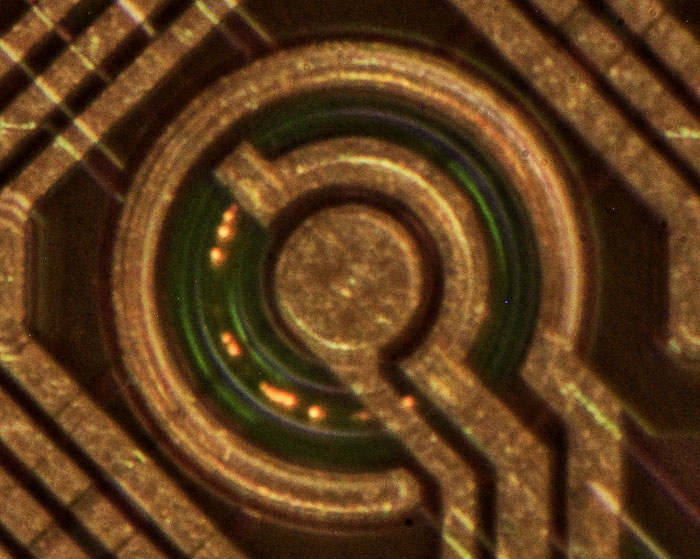
https://www.richis-lab.de/Transistoren.htmAnd I just have to show you this one:
You see the breakdown of the KD501-base-emitter-junction with increasing current.


Does anybody know why Tesla integrated this step at the edge of the die?
The BE breakdown video is great ?
I'm working on a PHD where this effect plays a role. May I use your video in my thesis ?
Just speculating, is this a MESA part ?
The BE breakdown video is great ?
I'm working on a PHD where this effect plays a role. May I use your video in my thesis ?
Thanks!
Of course you can use it in your PHD.
If you need something special (higher resolution, different angle,...) just tell me.
Just speculating, is this a MESA part ?
Sounds reasonable!

Just speculating, is this a MESA part ?
Sounds reasonable!
Looks exactly as on book drawings

... just a question - is the 2N2222A also emitting light in BE breakdown ?
regards
Wolfgang
Is it possible to check tip3055 and tip2955 from onsemi and st? I'm willing to sponsor this. They are in plastic enclosure, to-264 or to-247.
... just a question - is the 2N2222A also emitting light in BE breakdown ?
regards
Wolfgang
I´m pretty sure every bipolar transistor has the same glowing.
I want to do this again with a smaller transistor. Let´s see what I have on my bench.
Is it possible to check tip3055 and tip2955 from onsemi and st? I'm willing to sponsor this. They are in plastic enclosure, to-264 or to-247.
In principle that´s no problem:
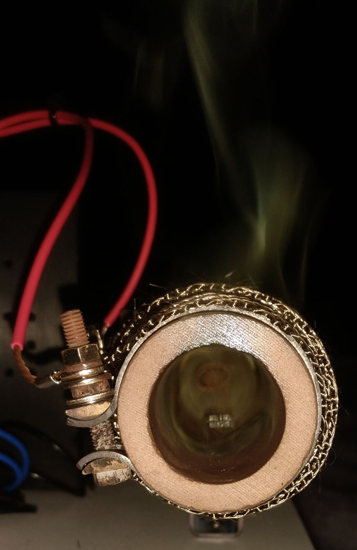 https://www.richis-lab.de/decap-ofen.htm
 My success rate is something around 95%. Only very few package fail in decapping but there are some.
And it takes some days. After all it´s only a hobby.

If that´s ok for you feel free to send me the parts.
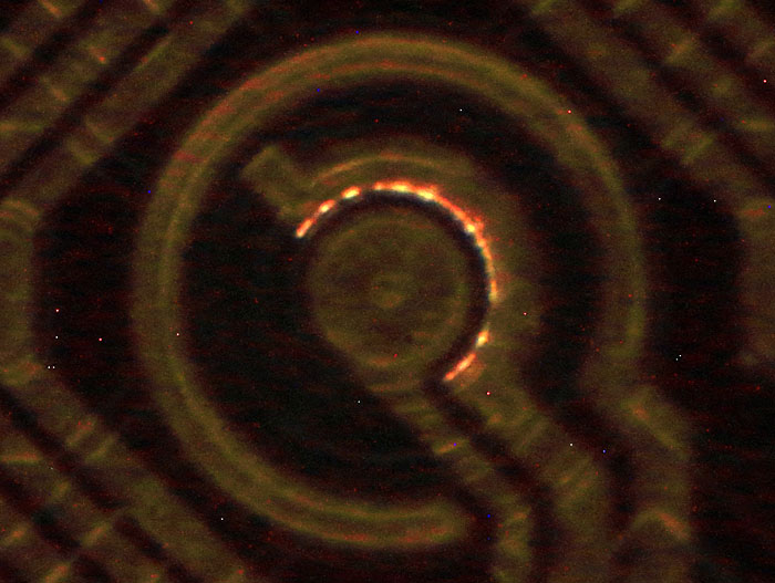
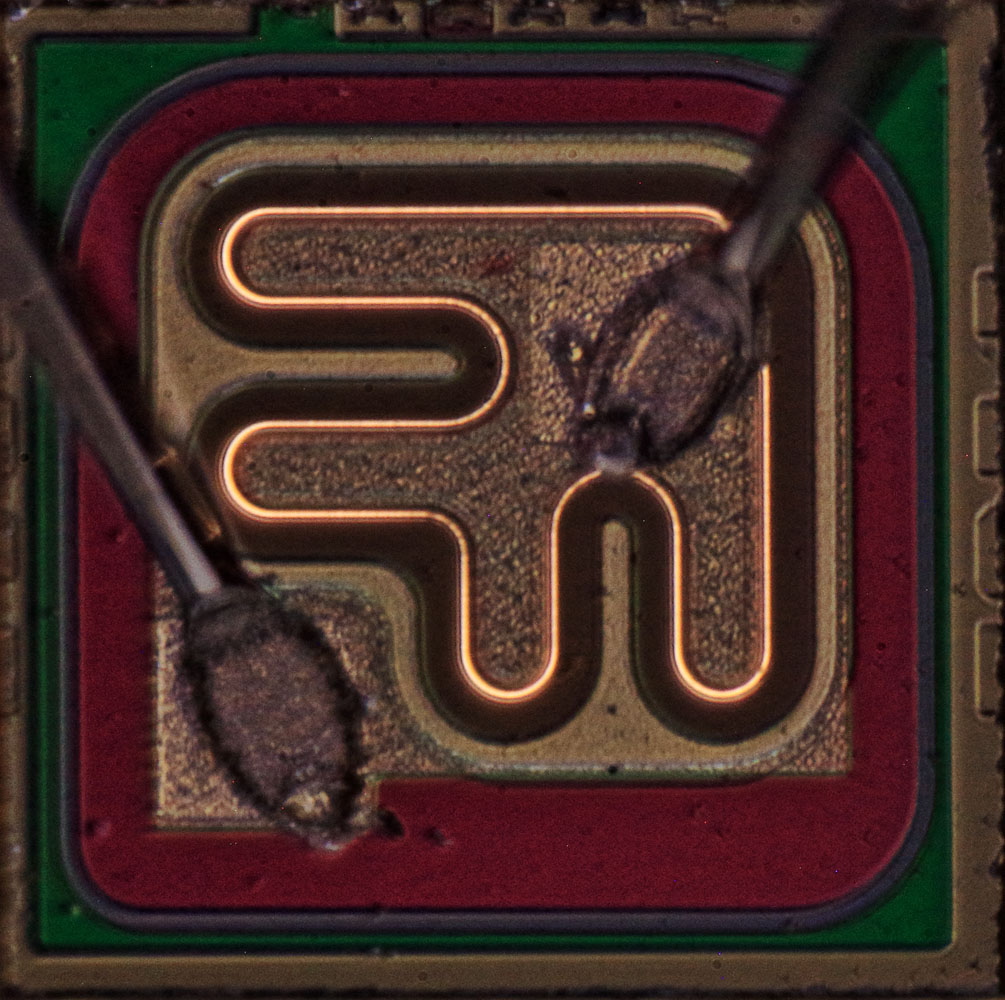
I have uploaded a new row of pictures including the current values:
https://www.richis-lab.de/Bipolar02.htmOne interesting effect is the positive temperature coefficient of the breakdown voltage (Z-diode with Vbr=10V). If you connect a voltage at B-E that is just high enough to let it break down and then increase the current the B-E-junction suddenly gets non conductive again. => Physics!
I have uploaded a new row of pictures including the current values:
https://www.richis-lab.de/Bipolar02.htm
One interesting effect is the positive temperature coefficient of the breakdown voltage (Z-diode with Vbr=10V). If you connect a voltage at B-E that is just high enough to let it break down and then increase the current the B-E-junction suddenly gets non conductive again. => Physics!
Very interesting results with the optical output from the reversed breakdown EB junction!!
Also like the method you've developed to de-encapsulate ICs based upon "burning" off the epoxy, very clever
An interesting effect on some bipolar transistors when used with EB junction reversed biased in this type behavior where the plot of voltage vs. current has a region of negative slope when entering breakdown, or dV/dI is negative, thus negative resistance. This is the type of behavior of a avalanche or tunnel diode.
One can build a simple "relaxation oscillator" by using a large (~100K) resistor to supply a higher than breakdown voltage (usually >10 volts) to the Emitter junction of an NPN transistor. The base is ground and collector open (also try a connect to collector ground and leave the base open), a capacitor (10nF) shunting the EB junction to ground. With a scope you can observe a sawtooth relaxation waveform across the EB junction as you adjust the supply voltage. This waveform is caused by the charging of the capacitor with the RC time constant, then a rapid discharge as the junction enters the negative resistance region, then a repeat of this cycle.
The late Jim Williams (brilliant analog engineer, RIP) discussed at the ISSCC awhile back (I had a brief private discussion with him) how he designed a cheap voltage reference using a small NPN transistor with the EB junction operated in breakdown which produces a positive TC, then the base was left open and the collector grounded. This would forward bias the base to collector diode would produce the negative TC compensating the positive TC of the reversed breakdown of the EB junction. This went into production only to find that the composite transistor based reference was oscillating using the decoupling capacitor and resistor bias!!
Best,
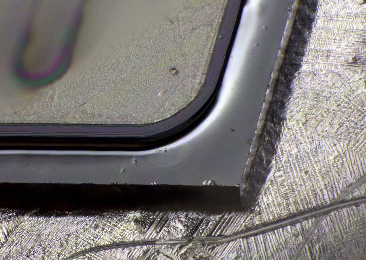
Today I have a Germanium-Transistor for you, a Philips AU301:
https://www.richis-lab.de/Bipolar03.htm
It´s an alloy transistor. The combination of power and alloy transistor leads to an interesting design...
There are spots that light up first. Are those the hot spots responsible for secondary breakdown?
No. Secondary breakdown occurs at the BC junction, not at BE.
You had a private discussion with Jim Williams? Very cool!
Yes, we talked briefly over coffee at the ISSCC in 2011 (Feb) and Jim passed away a few months later

Also had the pleasure of meeting and discussing things with Larry Nagle (Berkeley SPICE Author) at the ISSCC, a colleague worked with Larry at Bell Labs. Didn't make the ISSCC this year though, too risky.
BTW what current did you run thru the LTZ1000 to see the optical output? Would really like to get an LTZ1000, but they've become very expensive lately

Best,
BTW what current did you run thru the LTZ1000 to see the optical output? Would really like to get an LTZ1000, but they've become very expensive lately
I believe it was something around 10mA or 20mA back in the day.
The LTZ1000 was a noisy one a voltnut donated to me.
...I have a AD1139 on the bench…
... just a question - is the 2N2222A also emitting light in BE breakdown ?
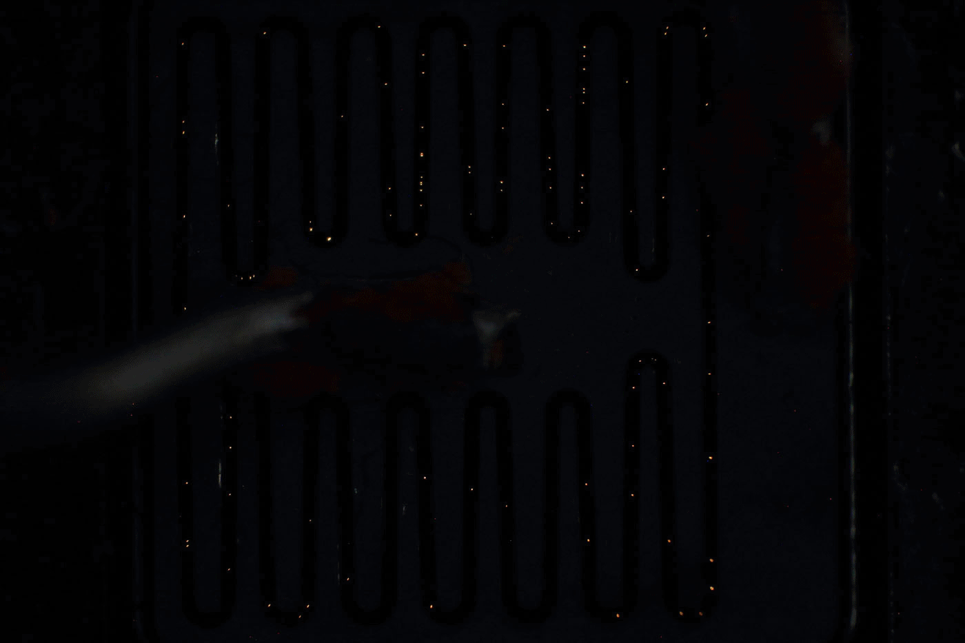
Coincidentally I had a 2N2222A in my inbox.
As expected the BE-junction glows too.
I then killed the 2N2222A and made a short video.

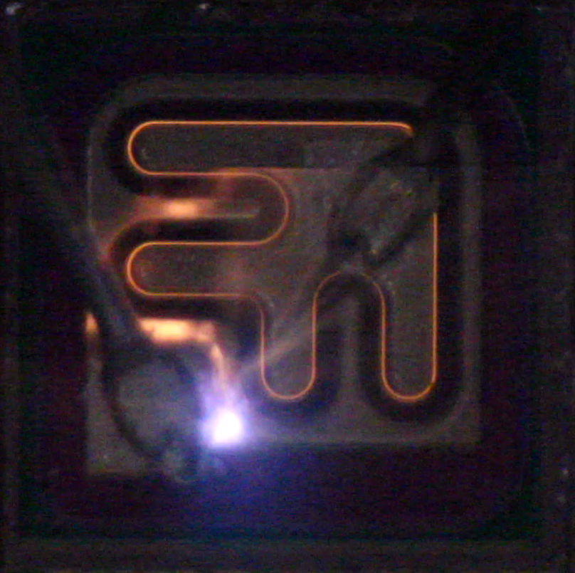
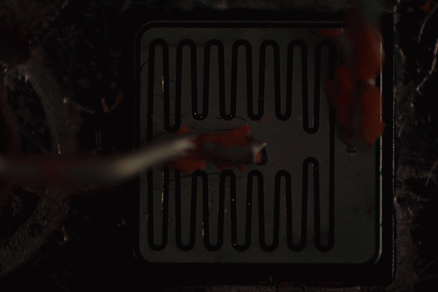
You can identify the route of destruction:
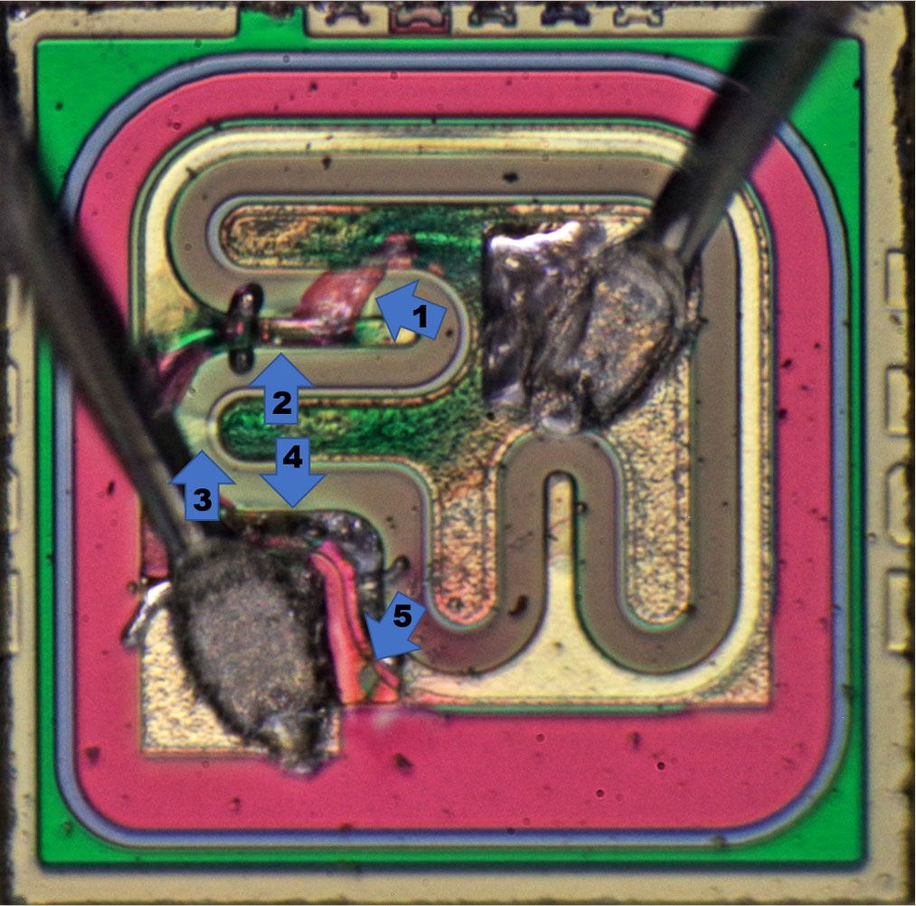
My Interpretation:
1) First
breakdown destruction of the BE-junction.
2) Base-Electrode melts and cuts the current.
3) Second destruction of the BE-junction.
4) Base-metal melts further to the bondpad.
5) Last connection is disrupted with a bright arc.
Interesting...

More pictures here:
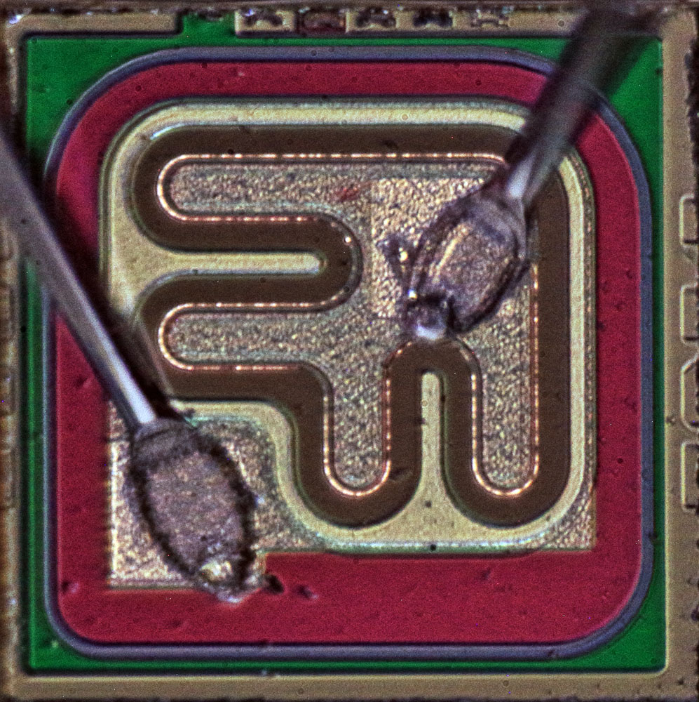
https://www.richis-lab.de/Bipolar04.htm
... just a question - is the 2N2222A also emitting light in BE breakdown ?
Coincidentally I had a 2N2222A in my inbox.
As expected the BE-junction glows too.
I then killed the 2N2222A and made a short video.
You can identify the route of destruction:
My Interpretation:
1) First breakdown destruction of the BE-junction.
2) Base-Electrode melts and cuts the current.
3) Second destruction of the BE-junction.
4) Base-metal melts further to the bondpad.
5) Last connection is disrupted with a bright arc.
Interesting...
More pictures here:
https://www.richis-lab.de/Bipolar04.htm
Rich, just awesome, just what I need ! Thanks a lot !
Some questions:
- the video shows a very fast current increase. Did you run this with a current source ? Or is just the video too fast ?
- In my transistors, I see a noise curve very explainable by your KD503 video. First, only a few hotspots light up,
then more and more, until the whole area is bright. So noise *falls* with rising current. The 2N2222 seems to start almost immediately. Why ?
The Zener range is the same (> 7V), so it must be an avalanche mechanism.
- Do you want noise plots ? In case the 2N2222A behaves the same, they could be of interest.
Thanks again ! If you dont mind, I really want to give you an honourable mention in a paper I'm writing.
- the video shows a very fast current increase. Did you run this with a current source ? Or is just the video too fast ?
The bench supply is the weak spot of my lab.

I used a very cheap supply for this experiment. In the video I just cranked up the current limit to overload the 2N2222. I assume the current jumped up to something around 200mA, didn´t check that.
In the meantime I have some HP-supplies but I still have to integrate them into my bench...
- In my transistors, I see a noise curve very explainable by your KD503 video. First, only a few hotspots light up,
then more and more, until the whole area is bright. So noise *falls* with rising current. The 2N2222 seems to start almost immediately. Why ?
The Zener range is the same (> 7V), so it must be an avalanche mechanism.
Why? My supply!
It´s a pain in the ass to adjust the current limit around 10mA. The supply doesn´t even show smaller currents than 10mA. I had to meassure the current with my bench meter.
In the KD503 10mA is low enough to get the small little hotspots. In the 2N2222 with 10mA the current density is already high enough to light it up almost completely.
I have uploaded a new picture showing the glowing with lower current:
You can see the light is not uniform. With smaller currents I´m sure it would look like the KD501.
I observed the same effect with the 2N3055:
To get a uniform light in the big old ones you need a lot of current. They get pretty hot. In the newer small dies some ten mA are enough to get a nice light all over the place.
- Do you want noise plots ? In case the 2N2222A behaves the same, they could be of interest.
Of course! That would be very interesting!
Thanks again ! If you dont mind, I really want to give you an honourable mention in a paper I'm writing.
It would be an honour!
I wonder if the glow pattern varies with charge state on the surface passivation (which is likely silica glass). This would be hard to test; perhaps exposed metal surfaces could be insulated with an insulating film, then a conductive liquid (e.g. salt water) applied to control the surface electric field? (Might need hundreds of volts, since the insulation will be so thick at this point.)
Tim
Why nobody put a photodiode inside to protect expensive power transistors?
I wonder if the glow pattern varies with charge state on the surface passivation (which is likely silica glass). This would be hard to test; perhaps exposed metal surfaces could be insulated with an insulating film, then a conductive liquid (e.g. salt water) applied to control the surface electric field? (Might need hundreds of volts, since the insulation will be so thick at this point.)
Tim
Possible but hard to test...

Why nobody put a photodiode inside to protect expensive power transistors?
In my view in real applications transistors rarely die because of base-emitter-breakdown.
Secondly you must be able to do something against the base-emitter-breakdown. Often base-emitter-breakdown occurs due to a bad design or a failure in an other circuit. It´s hard to compensate these things...
Why nobody put a photodiode inside to protect expensive power transistors?
... its not a real world problem for power parts. Any useful design prevents this, e.g. by an antiparallel diode at the base. Furthermore, you need quite some current to kill those parts.
The problem is more with small transistors, where a BE breakdown even with small currents and for short times only degrades gain at low currents permanently.
Hi Rich,
if you have no reliable constant current source you could try a normal power supply in constant voltage mode with a series resistor (or a pot) and a good multimeter in current mode. That should work.
Next week I could try to run this on a Keysight B2962 SMU.
Measured noise plot for 100uA, 1mA and 10mA is attached.
Best regards
Wolfgang
Hi Wolfgang,
I just have to power up my HP6627A. That should be sufficient. But it has binding posts on the back so I need some kind of a connection panel first.
The bench supply I use at the moment is ok (with a Fluke 45) but it´s definitely no SMU to specify semiconducter properties.
Thanks for the noise plots! Quite interesting!
Best regards,
Richard