Hi,
As the scope couldn´t measure in normal trigger mode, I´ve asked them if there will be any firmware upgrade in the future, to fix that.
This was on 13th august.
Today I receive an answer:
ReplyContent:
hi, friend
The situation you said is measurable, you can contact the store where you bought this product, and she will help you solve this problem. Thank you for your message and wish you a happy life!
ReplyDatetime:
2020-09-02 14:47
OK, I´m going to ask AMAZON... 
I was more than willing to pay $45 more and get mine from Amazon--I've been
banged good by a number of the online Asian vendors too many times to ever buy from them again. With AZ Prime, I received the instrument in 2 days as opposed to 2 months; and you simply have to say "I don't like it" and next thing you know you'll have a UPS return label and usually a refund within 1 hour of dropping the package off at UPS.
[How to fix irresponsive touchscreen] [with solution]
So I tried a couple of low value caps (1pF, 5pF, 10pF and 100pF) and they all made things a bit better, but the 100pF one made it just PERFECT  !
!
Maybe a bad cap in there? Did you measure it?
The soldering looks OK, but if it's a dud cap the QC (
) probably won't find such an issue.
Questions
1. Why is there a cap connected to SCL?
1.1 That's a capacitor, right?
2. Why is the cap connected across two signal lines?
2.1 I never saw anything like that in I2C lines, is this some advance hack?
2.2 What could the other signal be?
3. Why do you think the touchscreen was defective in the first place?
My Answers1. No idea
1.1. Certainly looks like it
2. No idea
2.1. Me either - maybe the touch controller datasheet had it in the reference design

2.2. Looks like SDA - based on the 2 pullup resistors
3. The capacitor plus pullup resistors that are too high in value would probably make the I2C signals a mess
In summaryThe cap appears to be placed across SDA and SCL. That makes pretty much no sense. You want minimal capacitance on those signals.
The two resistors would appear to be the I2C pullups, and have an EIA marking of "01C" or 10k. 10k is a bit too high for 3.3V I2C signals.
Around 3k3 would be better for 3.3V logic, with no additional capacitance.
A scope might be useful to check the signal integrity...

The cap appears to be placed across SDA and SCL. That makes pretty much no sense.
Maybe some intern added it because:
a) They have the wrong pullups
b) It didn't work reliably and kept locking up the I2C bus (because of A)
c) They had no clue about I2C (see point A) and by dumb luck the cap seemed to do
something (maybe it keeps the lines somewhere in the middle instead of them going all the way down to ground).
Around 3k3 would be better for 3.3V logic, with no additional capacitance.
Even that's a bit high, IMHO. I'd be looking under 1k.
maybe the touch controller datasheet had it in the reference design
Very doubtful.
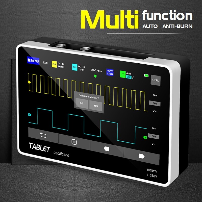
Still a dual channel 20MHz 7" touch screen portable tablet scope for $140 isn't bad.
I have buyed the 20MHz scope today.

I am a recent purchaser knowing that the specs were fantasy but so far I am well pleased with the device for the modest outlay.
One thing I am investigating is how to interpret the waveform .wav files as this can be useful for long term storage and further analysis on a computer. The aim is to write a script to transform the wav format into something more friendly like a spreadsheet or csv file. I am using intermediate versions of this to allow comparison between captures with different settings, data etc.
What I have discovered so far about the 15000 byte files is
0-999 Header data
1000 - 3999 CH1 data1
4000 - 6999 CH2 data1
7000 - 8499 CH1 data2
8500 - 9999 CH2 data2
10000 - 14999 seems to be just nulls in my captures so far.
The header data
CH1 vertical scale at 4 where 0-6 represents 5.0V,2.5V,1.0V,500mV,200mV,100mV,50mV/div
CH2 vertical scale at 14 (same as CH1
Time scale at 22 (repeated at 52 where 0 - 29 represents
50S,20S,10S,5S,2S,1S,500mS,200mS,100mS,50mS,20mS,10ms,5mS,2mS,1mS,
500uS,200uS,100uS,50uS,20uS,10uS,5uS,2uS,1uS,500nS,200nS,100nS,50nS,20nS,10nS
Ch1 measurements at 208 - 255 (12 4byte fields)
Ch2 measurements at 256 - 303 (12 4byte fields)
Ch dataBlock1 1500 2 byte fields (little endian) which represent in some way the vertical measurement on the screen. I.e. doubling sensitivity doubles the values in this block.
I would be interested if anybody has any knowledge or insights in this area e.g. similarity to other formats, so I can avoid unnecessary work.
My current investigation is focussed on two area.
1) The representation of the data in dataBlocks1 and 2 in order to be able to transform it into 'real data'
2) The mapping of the measurement data regions on to the parameters and the encoding used in each 4 byte value. I have an inkling that the first byte is a type indicator and the next 3 are little endian values (maybe fixed point).
I'd guess 'data1' is the raw sample data and 'data2' is what's shown on screen (double the number of horizontal pixels is quite common in 'scopes)
Thanks.
Yes, that does seem to be the case for DataBlock2. If I compare a .bmp which is 800x400 it shows the active screen area as 750 pixels wide. The DataBlock2 is then the Y offset from the top of the screen for each of the 750 X positions.
The divisions on the screen are 50x50px so one could crudely extract values from the dataBlock2. More interesting is to use the values from DataBlock1 as that gives the full buffer.
The values in DataBlock1 do not appear to be raw ADC values but seem to follow the same scale as the values in DataBlock2 but with a different baseline. E.g large square wave in DataBlock1 might have values 79 -> 391 corresponding to values 370 -> 58 in DataBlock2. Values are vertically mirroed as one might expect.
So I think DataBlock1 has been scaled to represent 50 / div. There are probably values in the hdr which give the baselines used> There will also be values giving things like vertical and horizontal offsets, trigger level etc. plus all other settings.
One trick they missed was allowing run after restoring a waveform as that would have been a neat way of saving / restoring setups.
The values in DataBlock1 do not appear to be raw ADC values but seem to follow the same scale as the values in DataBlock2 but with a different baseline.
ADC values are often scaled and only use 200 of the 256 available values when the screen is 400-pixels tall. This way there's a simple 2:1 mapping of values to screen pixels.
eg. The Rigol DS1054Z does this and I'm sure many others do, too.
Why? I think it's just to avoid doing a divide in the screen display functions (which would be needed if all 256 values were used).
Thanks.
The data buffer readings range 0 - 399 with 200 corresponding to 0. So with a 1V/div then 100 corresponds to -2.0V and 300 corresponds to +2.0V
However, it doesn't seem to be pure pixel doubling from an ADC range of 200 as both even and odd values appear in the buffer. E.g the top of a square wave can have values varying by 1.
I should be able to make a conversion that at least contains sensible data. I am working my way through capturing different settings like trigger so I can see how they are represented in the buffer.
he data buffer readings range 0 - 399 with 200 corresponding to 0
They're 16-bits but only using 9 of them? That seems a bit of a waste.
IOW data1 is a 16-bit version of data2? 3000 bytes instead of 1500 bytes?
However, it doesn't seem to be pure pixel doubling from an ADC range of 200 as both even and odd values appear in the buffer. E.g the top of a square wave can have values varying by 1.
Maybe it's had sin(x)/x applied to it (or some other filter).
I think the use of 16 bit values is just because the numbers won't fit into 1 byte.
DataBlock2 is still 16 bit values but just showing the 750 display values instead of the 1500 values in the buffer.
I have updated further with latest results of investigation into header values with scope settings. Measures is still to be sorted out. Values need to have probe multiplier factored in.
I am keeping stuff including a test script at
https://github.com/roberttidey/FNISR1013DScope
I have now added onto the repository a python program FNISR1013D-JSON.py
When run it asks for a filename; enter the root filename of a wav file (e.g 9 for 9.wav). It will produce json file (9.json) containing the buffer and display data plus settings for the capture. The json format makes it easy to access the data.
Measures remain a work in progress as I have to figure out the encoding and mapping of the 24 byte measure fields.
Mapping of measures onto header values is now added to the waveform file converter (python)
Most values seem Ok except for cycle and time+/- and I can't see at the moment how negative voltages are indicated. There is also appears to be a calibration factor for adjusting volates which may be in the header somewhere.
The negative sign for voltage measures does not seem to be stored in the waveform file.
When a waveform capture is done then the absolute value is stored but when is restored then the signs of the values just pick up whatever the sign of the last live measurement was.
That's a bit of a drop off in the software.
It doesn't affect the data buffer values as they have an offset which effectively incorporates the sign.
By the time I would have order it, it was sold out, but I found another listing with the same price and I ordered it. We will see what is it
But in the meantime as I see they are changing back the pricing of the other listings to ~150USD

Is it a fake?
I don´t think it is.
It will be always the same hardware under different names = vendors.
My Fnirsi is a Yeapook..

Banggood sell both this one and the original one. They call this the "upgraded" version with the following improvements:
"Comparison between the new version and the previous version:
1. Product functions and parameters have not changed.
2. Replacement and improved appearance: the screen is replaced with a toughened glass screen, which is more wear-resistant and sturdy; the probe socket is also hidden, which is more beautiful. The overall appearance is more beautiful~"
So, if beauty is what you are after...
So, if beauty is what you are after...
(sorry for the extra post, but I had to react to this)
To me the case difference is probably that the original was supposed to have a boot. Curved corners unprotected power and BNC conns. The new case sinks the power switch and so on.
I bought this "new" version from Amazon Germany, and received it today. After using it for the first time, and saving one image and one waveform, this obviously damaged the internal SD image... Now I only get a red "SD ERROR" when switching on the device...
Here are some pictures:
https://photos.app.goo.gl/zzHKWVhr7CXszsA66Does anyone have a proper SD image for this device (FNRISI-1013D-II), that I can use to fix the device? Any help would be much appreciated!
Thank you very much & best regards from Vienna,
Markus
I bought this "new" version from Amazon Germany, and received it today. After using it for the first time, and saving one image and one waveform, this obviously damaged the internal SD image... Now I only get a red "SD ERROR" when switching on the device...
That might be coincidence, not cause/effect.
Does anyone have a proper SD image for this device (FNRISI-1013D-II), that I can use to fix the device? Any help would be much appreciated!
Could be a bad SD card, not fixable. Or maybe it just needs pulling out and putting back in again.
 The "specs" are the same, but the price is too good to be true